 | –≠–ª–µ–∫—Ç—Ä–æ–Ω–Ω—ã–π –∫–æ–º–ø–æ–Ω–µ–Ω—Ç: 29F800 | –°–∫–∞—á–∞—Ç—å:  PDF PDF  ZIP ZIP |
1/21
PRELIMINARY DATA
January 2000
This is preliminary information on a new product now in development or undergoing evaluation. Details are subject to change without notice.
M29F800AT
M29F800AB
8 Mbit (1Mb x8 or 512Kb x16, Boot Block)
Single Supply Flash Memory
s
SINGLE 5V
±
10% SUPPLY VOLTAGE for
PROGRAM, ERASE and READ OPERATIONS
s
ACCESS TIME: 70ns
s
PROGRAMMING TIME
≠ 8
µ
s per Byte/Word typical
s
19 MEMORY BLOCKS
≠ 1 Boot Block (Top or Bottom Location)
≠ 2 Parameter and 16 Main Blocks
s
PROGRAM/ERASE CONTROLLER
≠ Embedded Byte/Word Program algorithm
≠ Embedded Multi-Block/Chip Erase algorithm
≠ Status Register Polling and Toggle Bits
≠ Ready/Busy Output Pin
s
ERASE SUSPEND and RESUME MODES
≠ Read and Program another Block during
Erase Suspend
s
TEMPORARY BLOCK UNPROTECTION
MODE
s
LOW POWER CONSUMPTION
≠ Standby and Automatic Standby
s
100,000 PROGRAM/ERASE CYCLES per
BLOCK
s
20 YEARS DATA RETENTION
≠ Defectivity below 1 ppm/year
s
ELECTRONIC SIGNATURE
≠ Manufacturer Code: 0020h
≠ M29F800AT Device Code: 00ECh
≠ M29F800AB Device Code: 0058h
44
1
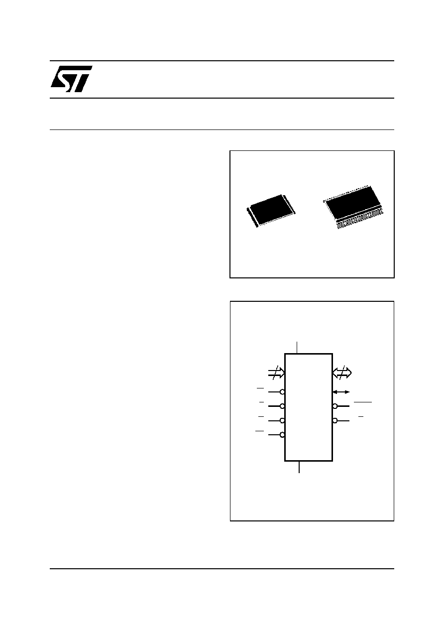
TSOP48 (N)
12 x 20mm
SO44 (M)
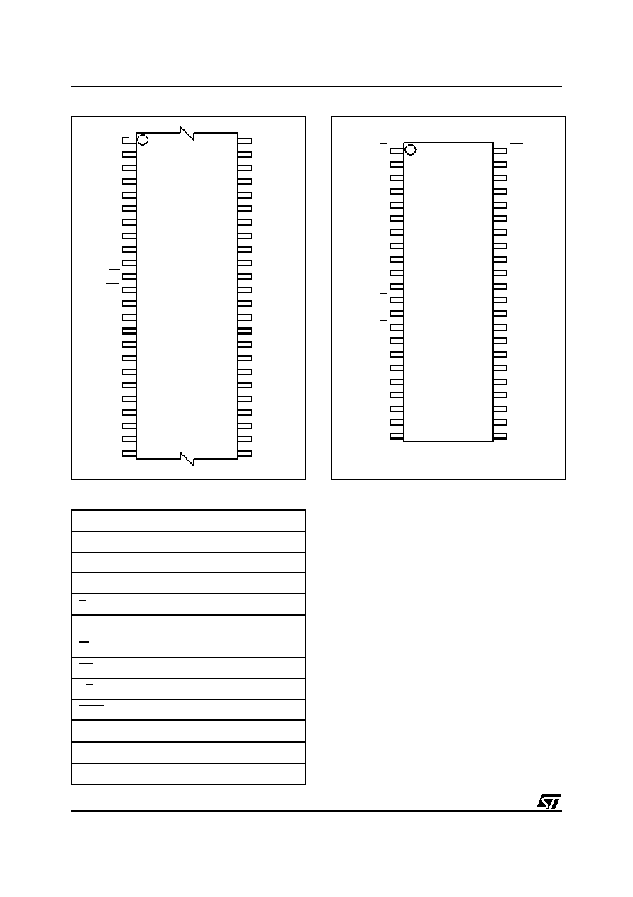
Figure 1. Logic Diagram
AI02198B
19
A0-A18
W
DQ0-DQ14
VCC
M29F800AT
M29F800AB
E
VSS
15
G
RP
DQ15A≠1
BYTE
RB
M29F800AT, M29F800AB
2/21
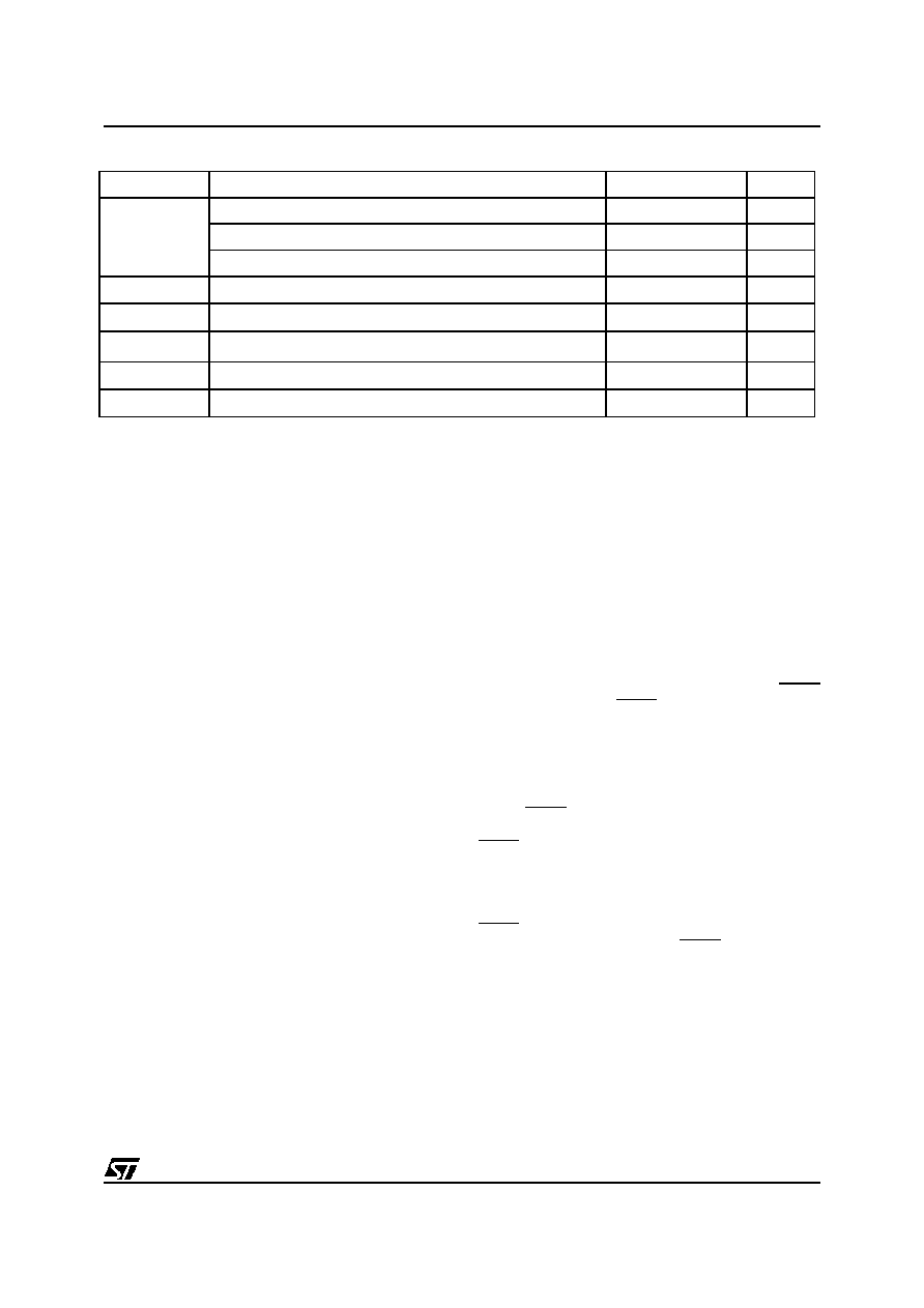
Figure 2A. TSOP Connections
DQ3
DQ9
DQ2
DQ0
DQ6
DQ13
DQ14
DQ12
DQ10
DQ15A≠1
VCC
DQ4
DQ5
DQ7
AI02199
M29F800AT
M29F800AB
12
1
13
24
25
36
37
48
DQ8
DQ1
DQ11
A16
BYTE
VSS
A0
VSS
A6
A3
A8
A9
A17
A10
A2
A7
NC
NC
NC
NC
A1
A18
A4
A5
A12
A13
A11
A15
A14
RP
W
RB
G
E
Table 1. Signal Names
A0-A18
Address Inputs
DQ0-DQ7
Data Inputs/Outputs
DQ8-DQ14
Data Inputs/Outputs
DQ15A≠1
Data Input/Output or Address Input
E
Chip Enable
G
Output Enable
W
Write Enable
RP
Reset/Block Temporary Unprotect
RB
Ready/Busy Output
BYTE
Byte/Word Organization Select
V
CC
Supply Voltage
V
SS
Ground
NC
Not Connected Internally
SUMMARY DESCRIPTION
The M29F800A is an 8 Mbit (1Mb x8 or 512Kb
x16) non-volatile memory that can be read, erased
and reprogrammed. These operations can be per-
formed using a single 5V supply. On power-up the
memory defaults to its Read mode where it can be
read in the same way as a ROM or EPROM.
The memory is divided into blocks that can be
erased independently so it is possible to preserve
valid data while old data is erased. Each block can
be protected independently to prevent accidental
Program or Erase commands from modifying the
memory. Program and Erase commands are writ-
ten to the Command Interface of the memory. An
on-chip Program/Erase Controller simplifies the
process of programming or erasing the memory by
taking care of all of the special operations that are
required to update the memory contents. The end
of a program or erase operation can be detected
and any error conditions identified. The command
set required to control the memory is consistent
with JEDEC standards.
Figure 2B. SO Connections
G
DQ0
DQ8
A3
A0
E
VSS
A2
A1
A13
VSS
A14
A15
DQ7
A12
A16
BYTE
DQ15A≠1
DQ5
DQ2
DQ3
VCC
DQ11
DQ4
DQ14
A9
W
RB
A4
A18
RP
A7
AI02101B
M29F800AT
M29F800AB
8
2
3
4
5
6
7
9
10
11
12
13
14
15
16
32
31
30
29
28
27
26
25
24
23
22
20
19
18
17
DQ1
DQ9
A6
A5
DQ6
DQ13
44
39
38
37
36
35
34
33
A11
A10
DQ10
21
DQ12
40
43
1
42
41
A17
A8
3/21
M29F800AT, M29F800AB
The blocks in the memory are asymmetrically ar-
ranged, see Tables 3A and 3B, Block Addresses.
The first or last 64 Kbytes have been divided into
four additional blocks. The 16 Kbyte Boot Block
can be used for small initialization code to start the
microprocessor, the two 8 Kbyte Parameter
Blocks can be used for parameter storage and the
remaining 32K is a small Main Block where the ap-
plication may be stored.
Chip Enable, Output Enable and Write Enable sig-
nals control the bus operation of the memory.
They allow simple connection to most micropro-
cessors, often without additional logic.
The memory is offered in TSOP48 (12 x 20mm)
and SO44 packages. Access times of 70ns and
90ns are available. The memory is supplied with
all the bits erased (set to '1').
SIGNAL DESCRIPTIONS
See Figure 1, Logic Diagram, and Table 1, Signal
Names, for a brief overview of the signals connect-
ed to this device.
Address Inputs (A0-A18). The Address Inputs
select the cells in the memory array to access dur-
ing Bus Read operations. During Bus Write opera-
tions they control the commands sent to the
Command Interface of the internal state machine.
Data Inputs/Outputs (DQ0-DQ7). The Data In-
puts/Outputs output the data stored at the selected
address during a Bus Read operation. During Bus
Write operations they represent the commands
sent to the Command Interface of the internal state
machine.
Data Inputs/Outputs (DQ8-DQ14). The Data In-
puts/Outputs output the data stored at the selected
address during a Bus Read operation when BYTE
is High, V
IH
. When BYTE is Low, V
IL
, these pins
are not used and are high impedance. During Bus
Write operations the Command Register does not
use these bits. When reading the Status Register
these bits should be ignored.
Data Input/Output or Address Input (DQ15A-1).
When BYTE is High, V
IH
, this pin behaves as a
Data Input/Output pin (as DQ8-DQ14). When
BYTE is Low, V
IL
, this pin behaves as an address
pin; DQ15A≠1 Low will select the LSB of the Word
on the other addresses, DQ15A≠1 High will select
the MSB. Throughout the text consider references
to the Data Input/Output to include this pin when
BYTE is High and references to the Address In-
puts to include this pin when BYTE is Low except
when stated explicitly otherwise.
Table 2. Absolute Maximum Ratings
(1)
Note: 1. Except for the rating "Operating Temperature Range", stresses above those listed in the Table "Absolute Maximum Ratings" may
cause permanent damage to the device. These are stress ratings only and operation of the device at these or any other conditions
above those indicated in the Operating sections of this specification is not implied. Exposure to Absolute Maximum Rating condi-
tions for extended periods may affect device reliability. Refer also to the STMicroelectronics SURE Program and other relevant qual-
ity documents.
2. Minimum Voltage may undershoot to ≠2V during transition and for less than 20ns during transitions.
Symbol
Parameter
Value
Unit
T
A
Ambient Operating Temperature (Temperature Range Option 1)
0 to 70
∞
C
Ambient Operating Temperature (Temperature Range Option 6)
≠40 to 85
∞
C
Ambient Operating Temperature (Temperature Range Option 3)
≠40 to 125
∞
C
T
BIAS
Temperature Under Bias
≠50 to 125
∞
C
T
STG
Storage Temperature
≠65 to 150
∞
C
V
IO
(2)
Input or Output Voltage
≠0.6 to 6
V
V
CC
Supply Voltage
≠0.6 to 6
V
V
ID
Identification Voltage
≠0.6 to 13.5
V
M29F800AT, M29F800AB
4/21
Table 3A. M29F800AT Block Addresses
Size
(Kbytes)
Address Range
(x8)
Address Range
(x16)
16
FC000h-FFFFF h
7E000h-7FFFFh
8
FA000h-FBFFFh
7D000h-7DFFFh
8
F8000h-F9FFFh
7C000h-7CFFFh
32
F0000h-F7FFFh
78000h-7BFFFh
64
E0000h-EFFFF h
70000h-77FFFh
64
D0000h-DFFFFh
68000h-6FFFFh
64
C0000h-CFFFFh
60000h-67FFFh
64
B0000h-BFFFF h
58000h-5FFFFh
64
A0000h-AFFFF h
50000h-57FFFh
64
90000h-9FFFFh
48000h-4FFFFh
64
80000h-8FFFFh
40000h-47FFFh
64
70000h-7FFFFh
38000h-3FFFFh
64
60000h-6FFFFh
30000h-37FFFh
64
50000h-5FFFFh
28000h-2FFFFh
64
40000h-4FFFFh
20000h-27FFFh
64
30000h-3FFFFh
18000h-1FFFFh
64
20000h-2FFFFh
10000h-17FFFh
64
10000h-1FFFFh
08000h-0FFFFh
64
00000h-0FFFFh
00000h-07FFFh
Table 3B. M29F800AB Block Addresses
Size
(Kbytes)
Address Range
(x8)
Address Range
(x16)
64
F0000h-FFFFF h
78000h-7FFFFh
64
E0000h-EFFFFh
70000h-77FFFh
64
D0000h-DFFFF h
68000h-6FFFFh
64
C0000h-CFFFF h
60000h-67FFFh
64
B0000h-BFFFFh
58000h-5FFFFh
64
A0000h-AFFFFh
50000h-57FFFh
64
90000h-9FFFFh
48000h-4FFFFh
64
80000h-8FFFFh
40000h-47FFFh
64
70000h-7FFFFh
38000h-3FFFFh
64
60000h-6FFFFh
30000h-37FFFh
64
50000h-5FFFFh
28000h-2FFFFh
64
40000h-4FFFFh
20000h-27FFFh
64
30000h-3FFFFh
18000h-1FFFFh
64
20000h-2FFFFh
10000h-17FFFh
64
10000h-1FFFFh
08000h-0FFFFh
32
08000h-0FFFFh
04000h-07FFFh
8
06000h-07FFFh
03000h-03FFFh
8
04000h-05FFFh
02000h-02FFFh
16
00000h-03FFFh
00000h-01FFFh
Chip Enable (E). The Chip Enable, E, activates
the memory, allowing Bus Read and Bus Write op-
erations to be performed. When Chip Enable is
High, V
IH
, all other pins are ignored.
Output Enable (G). The Output Enable, G, con-
trols the Bus Read operation of the memory.
Write Enable (W). The Write Enable, W, controls
the Bus Write operation of the memory's Com-
mand Interface.
Reset/Block Temporary Unprotect (RP). The Re-
set/Block Temporary Unprotect pin can be used to
apply a Hardware Reset to the memory or to tem-
porarily unprotect all blocks that have been pro-
tected.
A Hardware Reset is achieved by holding Reset/
Block Temporary Unprotect Low, V
IL
, for at least
t
PLPX
. After Reset/Block Temporary Unprotect
goes High, V
IH
, the memory will be ready for Bus
Read and Bus Write operations after t
PHEL
or
t
RHEL
, whichever occurs last. See the Ready/Busy
Output section, Table 14 and Figure 10, Reset/
Temporary Unprotect AC Characteristics for more
details.
Holding RP at V
ID
will temporarily unprotect the
protected blocks in the memory. Program and
Erase operations on all blocks will be possible.
The transition from V
IH
to V
ID
must be slower than
t
PHPHH
.
Ready/Busy Output (RB). The Ready/Busy pin
is an open-drain output that can be used to identify
when the memory array can be read. Ready/Busy
is high-impedance during Read mode, Auto Select
mode and Erase Suspend mode.
After a Hardware Reset, Bus Read and Bus Write
operations cannot begin until Ready/Busy be-
comes high-impedance. See Table 14 and Figure
10, Reset/Temporary Unprotect AC Characteris-
tics.
During Program or Erase operations Ready/Busy
is Low, V
OL
. Ready/Busy will remain Low during
Read/Reset commands or Hardware Resets until
the memory is ready to enter Read mode.
The use of an open-drain output allows the Ready/
Busy pins from several memories to be connected
to a single pull-up resistor. A Low will then indicate
that one, or more, of the memories is busy.
Byte/Word Organization Select (BYTE). The Byte/
Word Organization Select pin is used to switch be-
tween the 8-bit and 16-bit Bus modes of the mem-
ory. When Byte/Word Organization Select is Low,
V
IL
, the memory is in 8-bit mode, when it is High,
V
IH
, the memory is in 16-bit mode.
5/21
M29F800AT, M29F800AB
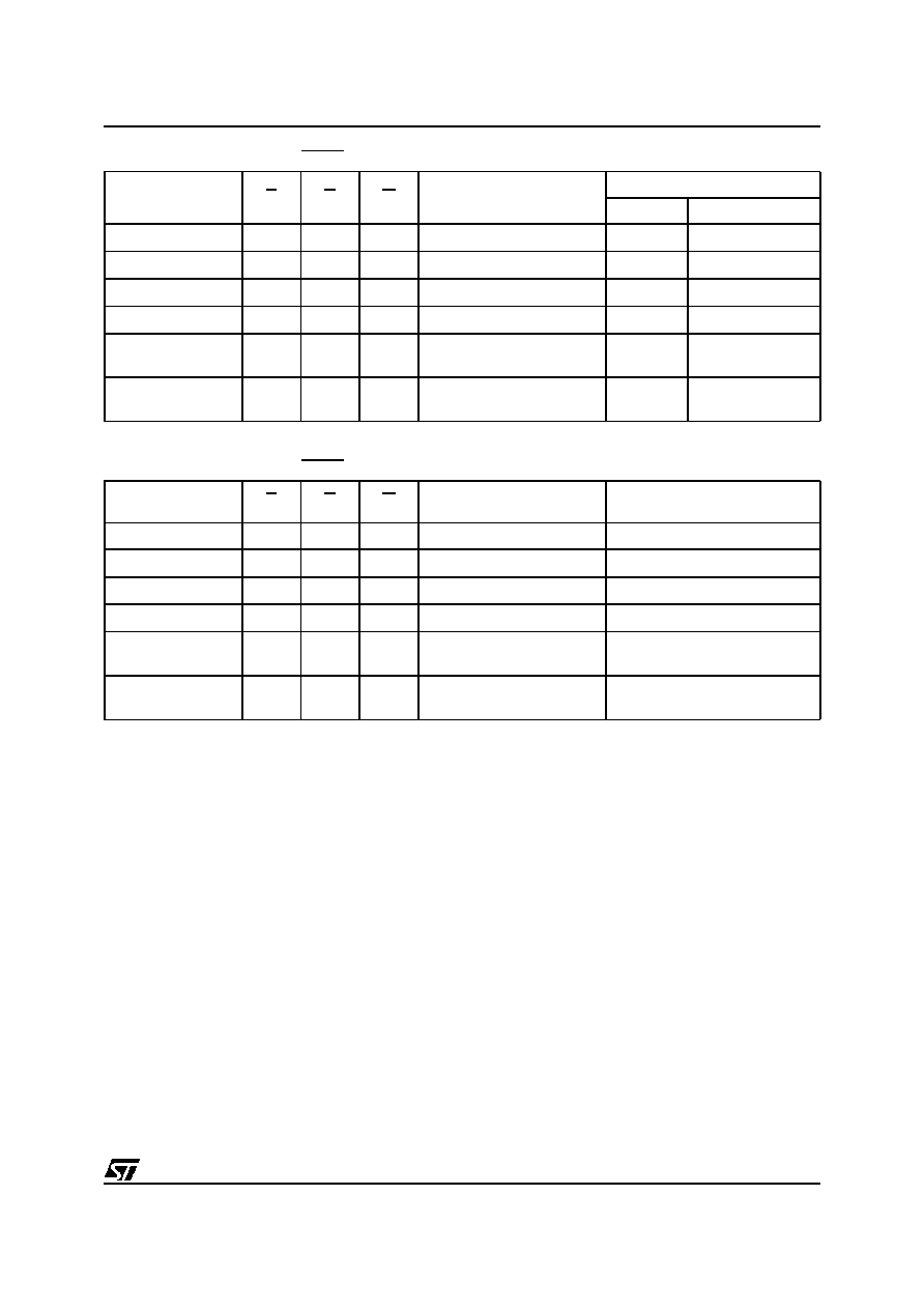
Table 4A. Bus Operations, BYTE = V
IL
Note: X = V
IL
or V
IH
.
Table 4B. Bus Operations, BYTE = V
IH
Note: X = V
IL
or V
IH
.
Operation
E
G
W
Address Inputs
DQ15A≠1, A0-A18
Data Inputs/Outpu ts
DQ14-DQ8
DQ7-DQ0
Bus Read
V
IL
V
IL
V
IH
Cell Address
Hi-Z
Data Output
Bus Write
V
IL
V
IH
V
IL
Command Address
Hi-Z
Data Input
Output Disable
X
V
IH
V
IH
X
Hi-Z
Hi-Z
Standby
V
IH
X
X
X
Hi-Z
Hi-Z
Read Manufacturer
Code
V
IL
V
IL
V
IH
A0 = V
IL
, A1 = V
IL
, A9 = V
ID
,
Others V
IL
or V
IH
Hi-Z
20h
Read Device Code
V
IL
V
IL
V
IH
A0 = V
IH
, A1 = V
IL
, A9 = V
ID
,
Others V
IL
or V
IH
Hi-Z
ECh (M29F800AT)
58h (M29F800AB)
Operation
E
G
W
Address Inputs
A0-A18
Data Inputs/Outpu ts
DQ15A≠1, DQ14-DQ0
Bus Read
V
IL
V
IL
V
IH
Cell Address
Data Output
Bus Write
V
IL
V
IH
V
IL
Command Address
Data Input
Output Disable
X
V
IH
V
IH
X
Hi-Z
Standby
V
IH
X
X
X
Hi-Z
Read Manufacturer
Code
V
IL
V
IL
V
IH
A0 = V
IL
, A1 = V
IL
, A9 = V
ID
,
Others V
IL
or V
IH
0020h
Read Device Code
V
IL
V
IL
V
IH
A0 = V
IH
, A1 = V
IL
, A9 = V
ID
,
Others V
IL
or V
IH
00ECh (M29F800AT)
0058h (M29F800AB)
V
CC
Supply Voltage. The V
CC
Supply Voltage
supplies the power for all operations (Read, Pro-
gram, Erase etc.).
The Command Interface is disabled when the V
CC
Supply Voltage is less than the Lockout Voltage,
V
LKO
. This prevents Bus Write operations from ac-
cidentally damaging the data during power up,
power down and power surges. If the Program/
Erase Controller is programming or erasing during
this time then the operation aborts and the memo-
ry
contents
being
altered
will
be
invalid.
A 0.1
µ
F capacitor should be connected between
the V
CC
Supply Voltage pin and the V
SS
Ground
pin to decouple the current surges from the power
supply. The PCB track widths must be sufficient to
carry the currents required during program and
erase operations, I
CC4
.
V
SS
Ground. The V
SS
Ground is the reference for
all voltage measurements.
BUS OPERATIONS
There are five standard bus operations that control
the device. These are Bus Read, Bus Write, Out-
put Disable, Standby and Automatic Standby. See
Tables 4A and 4B, Bus Operations, for a summa-
ry. Typically glitches of less than 5ns on Chip En-
able or Write Enable are ignored by the memory
and do not affect bus operations.
Bus Read. Bus Read operations read from the
memory cells, or specific registers in the Com-
mand Interface. A valid Bus Read operation in-
volves setting the desired address on the Address
Inputs, applying a Low signal, V
IL
, to Chip Enable
and Output Enable and keeping Write Enable
High, V
IH
. The Data Inputs/Outputs will output the
value, see Figure 7, Read Mode AC Waveforms,
and Table 11, Read AC Characteristics, for details
of when the output becomes valid.
Bus Write. Bus Write operations write to the
Command Interface. A valid Bus Write operation
begins by setting the desired address on the Ad-