2N3725
January 1989
HIGH VOLTAGE, HIGH CURRENT SWITCH
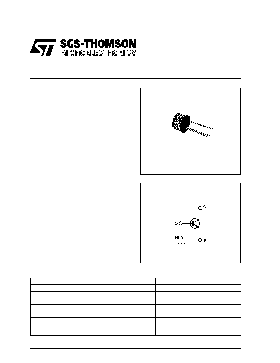
The 2N3725 is a silicon planar epitaxial transistor
in TO-39 metal case It is a high-voltage, high current
switch used for memory applications requiring
breakdown voltages up to 50 V and operating cur-
rents to 1 A. Fast switching times are assured be-
cause of the high minimum f
T
(300 MHz) and tight
control on storage time.
ABSOLUTE MAXIMUM RATINGS
Symbol
Parameter
Val ue
Unit
V
CBO
Collector-base Voltage (I
E
= 0)
80
V
V
CES
Collector-emitter Voltage (V
BE
= 0)
80
V
V
CEO
Collector-emitter Voltage (I
B
= 0)
50
V
V
EBO
Emitter-base Voltage (I
C
= 0)
6
V
I
C
Collector Current
1
A
P
t o t
Total Power Dissipation at T
amb
25
�
C
at T
c as e
25
�
C
0.8
3.5
W
W
T
s t g
, T
j
Storage and Junction Temperature
� 65 to 200
�
C
DESCRIPTION
TO-39
INTERNAL SCHEMATIC DIAGRAM
1/6

ELECTRICAL CHARACTERISTICS (T
amb
= 25
�
C unless otherwise specified)
Symbol
Parameter
Test Conditions
Min.
Typ.
Max.
Unit
I
CBO
Collector Cutoff Current (I
E
= 0)
V
CB
= 60 V
V
CB
= 60 V
T
am b
= 100
�
C
1.7
120
�
A
�
A
V(
B R)CBO
Collector-base Breakdown
Voltage (I
E
= 0)
I
C
= 10
�
A
80
V
V
(BR)CES
Collector-emitter Breakdown
Voltage (V
B E
= 0)
I
C
= 10
�
A
80
V
V(
BR)CE O
*
Collector-emitter Breakdown
Voltage (I
B
= 0)
I
C
= 10 mA
50
V
V(
B R)E BO
Emitter-base Breakdown
Voltage (I
C
= 0)
I
E
= 10
�
A
6
V
V
CE (s at )
*
Collector-emitter Saturation
Voltage
I
C
= 10 mA
I
C
= 100 mA
I
C
= 300 mA
I
C
= 500 mA
I
C
= 800 mA
I
C
= 1000 mA
I
B
= 1 mA
I
B
= 10 mA
I
B
= 30 mA
I
B
= 50 mA
I
B
= 80 mA
I
B
= 100 mA
0.19
0.21
0.31
0.4
0.5
0.6
0.25
0.26
0.4
0.52
0.8
0.95
V
V
V
V
V
V
V
BE (s at )
*
Base-emitter Saturation Voltage
I
C
= 10 mA
I
C
= 100 mA
I
C
= 300 mA
I
C
= 500 mA
I
C
= 800 mA
I
C
= 1000 mA
I
B
= 1 mA
I
B
= 10 mA
I
B
= 30 mA
I
B
= 50 mA
I
B
= 80 mA
I
B
= 100 mA
0.9
0.64
0.75
0.89
1.0
1.1
0.76
0.86
1.1
1.2
1.5
1.7
V
V
V
V
V
V
h
F E
*
DC Current Gain
I
C
= 10 mA
I
C
= 100 mA
I
C
= 300 mA
I
C
= 1000 mA
I
C
= 800 mA
I
C
= 500 mA
V
CE
= 1 V
V
CE
= 1 V
V
CE
= 1 V
V
CE
= 5 V
V
CE
= 2 V
V
CE
= 1 V
30
60
40
25
20
35
60
90
60
65
40
150
h
f e
High Frequency Current Gain
I
C
= 50 mA
f = 100 MHz
V
CE
= 10 V
3
C
CB O
Collector-base Capacitance
I
E
= 0
f = 1 MHz
V
CB
= 10 V
10
pF
C
EB O
Emitter-base Capacitance
I
C
= 0
f = 1 MHz
V
CB
= 0.5 V
55
pF
t
o n
**
Turn-on Time
I
C
= 500 mA
I
B
= 50 mA
V
CC
= 30 V
35
ns
t
o f f
**
Turn off Time
I
C
= 500 mA
I
B1
= � I
B2
=
V
CC
= 30 V
50 mA
60
ns
* Pulsed : pulse duration = 300
�
s, duty cycle = 1 %.
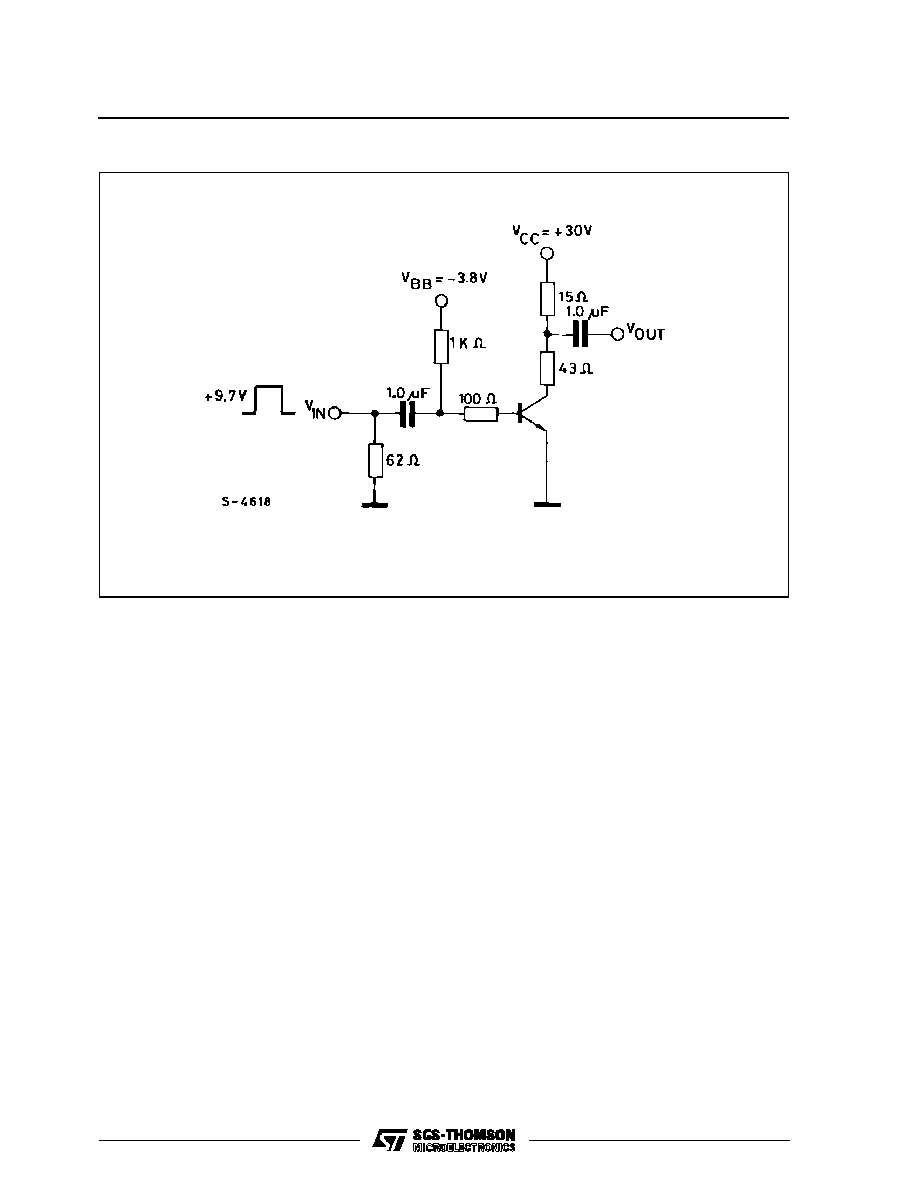
** See test circuit.
THERMAL DATA
R
t h j- cas e
R
t h j-amb
Thermal Resistance Junction-case
Thermal Resistance Junction-ambient
Max
Max
50
220
�
C/W
�
C/W
2N3725
2/6

DC Current Gain.
Collector-emitter Saturation Voltage.
Base-emitter Saturation Voltage.
Contours of Constant Transition Frequency.
Switching Characteristics.
Switching Characteristics.
2N3725
3/6