 | –≠–ª–µ–∫—Ç—Ä–æ–Ω–Ω—ã–π –∫–æ–º–ø–æ–Ω–µ–Ω—Ç: 2N5657 | –°–∫–∞—á–∞—Ç—å:  PDF PDF  ZIP ZIP |

2N5657
SILICON NPN TRANSISTOR
s
SGS-THOMSON PREFERRED SALESTYPE
s
NPN TRANSISTOR
DESCRIPTION
The 2N5657 is a silicon epitaxial-base NPN
transistor in Jedec SOT-32 plastic package. It is
intended for use output amplifiers, low current,
high voltage converters and AC line relays.
INTERNAL SCHEMATIC DIAGRAM
June 1997
ABSOLUTE MAXIMUM RATINGS
Symbol
Parameter
Val ue
Uni t
V
CBO
Collect or-Base Voltage (I
E
= 0)
375
V
V
CEO
Collect or-Emitt er Voltage (I
B
= 0)
350
V
V
EBO
Emitt er-Base Voltage (I
C
= 0)
6
V
I
C
Collect or Current
0.5
A
I
CM
Collect or Peak Current
1
A
I
B
Base Current
0. 25
A
P
t ot
Total Dissipation at T
c
25
o
C
20
W
T
stg
St orage Temperature
-65 to 150
o
C
T
j
Max. Operating Junction Temperature
150
o
C
3
2
1
SOT-32
1/5
THERMAL DATA
R
t hj-ca se
Thermal Resistance Junction-case
Max
6.25
o
C/W
ELECTRICAL CHARACTERISTICS (T
case
= 25
o
C unless otherwise specified)
Symb ol
Parameter
Test Cond ition s
Mi n.
Typ .
Max.
Un it
I
CBO
Collect or Cut-off
Current (I
E
= 0)
V
CE
= 375 V
0.01
mA
I
CEV
Collect or Cut-off
Current (V
BE
= -1.5V)
V
CE
= 350 V
V
CE
= 250 V
T
c
= 100
o
C
0.1
1
mA
mA
I
CEO
Collect or Cut-off
Current (I
B
= 0)
V
CE
= 250 V
0.1
mA
I
EBO
Emitt er Cut-off Current
(I
C
= 0)
V
EB
= 6 V
0.01
mA
V
( BR)CEO
Collect or-Emitter
Breakdown Volt age
I
C
= 1 mA
350
V
V
CEO(sus )
Collect or-Emitter
Sustaining Voltage
I
C
= 100 mA
L = 50 mH
350
V
V
CE(sat )
Collect or-Emitter
Saturat ion Voltage
I
C
= 0. 1 A
I
B
= 10 mA
I
C
= 0. 25 A
I
B
= 25 mA
I
C
= 0. 5 A
I
B
= 0.1 A
1
2.5
10
V
V
V
V
BE
Base-Emitt er Voltage
I
C
= 0. 1 A
V
CE
= 10 V
1
V
h
FE
DC Current G ain
I
C
= 50 mA
V
CE
= 10 V
I
C
= 0. 1 A
V
CE
= 10 V
I
C
= 0. 25 A
V
CE
= 10 V
I
C
= 0. 5 A
V
CE
= 10 V
25
30
15
5
250
h
f e
Small Signal Current
Gain
I
C
= 0. 1 A
V
CE
= 10 V
f = 1KHz
20
f
T
Transit ion f requency
I
C
= 50 mA
V
CE
= 10 V
f =10MHz
10
MHz
C
CBO
Collect or Base
Capacitance
V
CB
= 10 V
f = 100KHz
25
pF
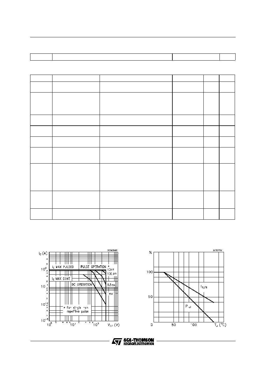
Pulsed: Pulse duration = 300
µ
s, duty cycle 1.5 %
Safe Operating Area
Derating Curve
2N5657
2/5

DC Current Gain (NPN type)
Collector Emitter Saturation Voltage (NPN type)
DC Current Gain (PNP type)
Collector Emitter Saturation Voltage (PNP type)
2N5657
3/5

DIM.
mm
inch
MIN.
TYP.
MAX.
MIN.
TYP.
MAX.
A
7.4
7.8
0.291
0.307
B
10.5
10.8
0.413
0.445
b
0.7
0.9
0.028
0.035
b1
0.49
0.75
0.019
0.030
C
2.4
2.7
0.040
0.106
c1
1.0
1.3
0.039
0.050
D
15.4
16.0
0.606
0.629
e
2.2
0.087
e3
4.15
4.65
0.163
0.183
F
3.8
0.150
G
3
3.2
0.118
0.126
H
2.54
0.100
H2
2.15
0.084
H2
0016114
SOT-32 (TO-126) MECHANICAL DATA
2N5657
4/5

Information furnished is believed to be accurate and reliable. However, SGS-THOMSON Microelectronics assumes no responsability for the
consequences of use of such information nor for any infringement of patents or other rights of third parties which may results from its use. No
license is granted by implication or otherwise under any patent or patent rights of SGS-THOMSON Microelectronics. Specifications mentioned
in this publication are subject to change without notice. This publication supersedes and replaces all information previously supplied.
SGS-THOMSON Microelectronics products are not authorized for use as critical components in life support devices or systems without express
written approval of SGS-THOMSON Microelectonics.
©
1997 SGS-THOMSON Microelectronics - Printed in Italy - All Rights Reserved
SGS-THOMSON Microelectronics GROUP OF COMPANIES
Australia - Brazil - Canada - China - France - Germany - Hong Kong - Italy - Japan - Korea - Malaysia - Malta - Morocco - The Netherlands -
Singapore - Spain - Sweden - Switzerland - Taiwan - Thailand - United Kingdom - U.S.A
. . .
2N5657
5/5