 | –≠–ª–µ–∫—Ç—Ä–æ–Ω–Ω—ã–π –∫–æ–º–ø–æ–Ω–µ–Ω—Ç: 68901P05 | –°–∫–∞—á–∞—Ç—å:  PDF PDF  ZIP ZIP |
MK68901
December 1988
MULTI≠FUNCTION PERIPHERAL
.
8 INPUT/OUTPUT PINS
∑
Individually programmable direction
∑
Individual interrupt source capability
-
Programmable edge selection
.
16 SOURCE INTERRUPT CONTROLLER
∑
8 Internal sources
∑
8 External sources
∑
Individual source enable
∑
Individual source masking
∑
Programmable interrupt service modes
-
Polling
-
Vector generation
-
Optional In-service status
∑
Daisy chaining capability
.
FOUR TIMERS WITH INDIVIDUALLY PRO-
GRAMMABLE PRESCALING
∑
Two multimode timers
-
Delay mode
-
Pulse width measurement mode
-
Event counter mode
∑
Two delay mode timers
∑
Independent clock input
∑
Time out output option
.
SINGLE CHANNEL USART
∑
Full Duplex
∑
Asynchronous to 65 kbps
∑
Byte synchronous to 1 Mbps
∑
Internal/External baud rate generation
∑
DMA handshake signals
∑
Modem control
∑
Loop back mode
.
68000 BUS COMPATIBLE
.
48 PIN DIP OR 52 PIN PLCC
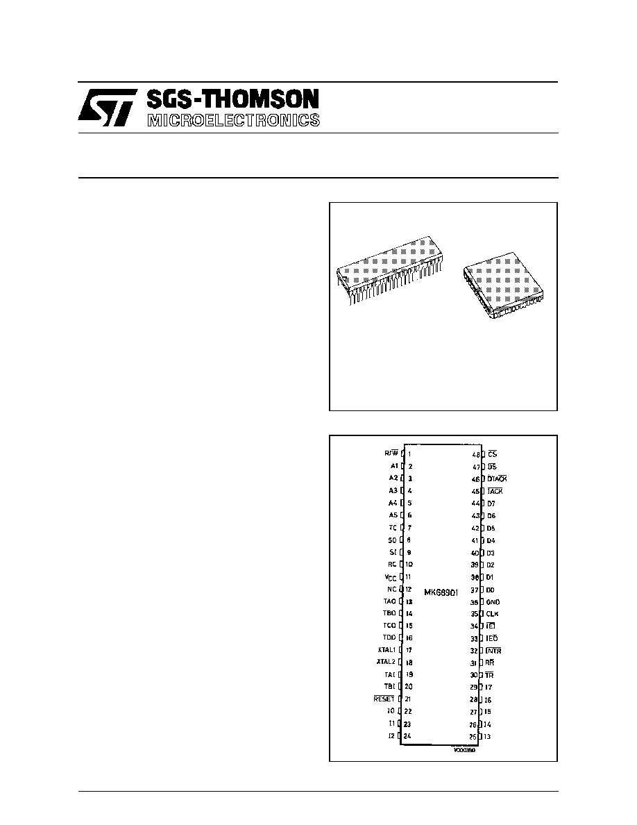
Figure 1 : Pin connections.
DESCRIPTION
The MK68901 MFP (Multi-Function Peripheral) is a
combination of many of the necessary peripheral
functions in a microprocessor system.
Included are :
Eight parallel I/O lines
Interrrupt controller for 16 sources
Four timers
Single channel full duplex USART
The use of the MFP in a system can significantly re-
duce chip count, thereby reducing system cost. The
MFP is completely 68000 bus compatible, and 24 di-
rectly addressable internal registers provide the ne-
MFP
1
DPIP48
PLCC52
1/33

necessary control and status interface to the pro-
grammer.
The MFP is a derivative of the MK3801 STI, a Z80
family peripheral.
PIN DESCRIPTION
GND :
Ground
V
CC
:
+5 volts (
±
5%)
CS :
Chip Select (input, active, low). CS is u-
sed to select the MK68901 MFP for ac-
cesses to the internal registers. CS and
IACK must not be asserted at the same
time.
DS :
Data Strobe (input, active low). DS is u-
sed as part of the chip select and interrupt
acknowledge functions.
R/W :
Read/Write (input). R/W is the signal
from the bus master indicating whether
the current bus cycle is a Read (High) or
Write (Low) cycle.
DTACK : Data Transfer Acknowledge. (output, ac-
tive low, tri-stateable) DTACK is used to
signal the bus master that data is ready,
or that data has been accepted by the
MK68901 MFP.
A1-A5 :
Address Bus (inputs). The adress bus is
used to adress one of the internal regis-
ters during a read or write cycle.
D0-D7 :
Data Bus (bi-directional, tri-stateable).
The data bus is used to receive data from
or transmit data to one of the internal re-
gisters during a read or write cycle. It is
also used to pass a vector during an in-
terrupt acknowledge cycle.
CLK :
Clock (input). This input is used to pro-
vide the internal timing for the MK68901
MFP.
RESET : Device reset. (input, active low). Reset
disables the USART receiver and trans-
mitter, stops all timers and forces the ti-
mer outputs low, disables all interrupt
channels and clears any pending inter-
rupts. The General Purpose Interrupt/I/O
lines will be placed in the tri-state input
mode. All internal registers (except the ti-
mer, USART data registers, and transmit
status register) will be cleared.
INTR :
Interrupt Request (output, active low, o-
pen drain). INTR is asserted when the
MK68901 MFP is requesting an interrupt.
INTR is negated during an interrupt ac-
knowledge cycle or by clearing the pen-
ding interrupt(s) through software.
IACK :
Interrupt Acknowledge (input, active
low). IACK is used to signal the MK68901
MFP that the CPU is acknowledging an
interrupt. CS and IACk must not be as-
serted at the same time.
IEI :
Interrupt Enable In (input, active low). IEI
is used to signal the MK68901 MFP that
no higher priority device is requesting in-
terrupt service.
IEO :
Interrupt Enable Out (output, active low).
IEO is used to signal lower priority peri-
pherals that neither the MK68901 MFP
nor another higher priority peripheral is
requesting interrupt service.
10-17 :
General Purpose Interrupt I/O lines.
These lines may be used as interrupt in-
puts and/or I/O lines. When used as in-
terrupt inputs, their active edge is pro-
grammable. A data direction register is u-
sed to define which lines are to be Hi-Z
inputs and which lines are to be push-pull
TTL compatible outputs.
SO :
Serial Output. This is the output of the U-
SART transmitter.
SI :
Serial Input. This is the input to the U-
SART receiver.
RC :
Receiver Clock. This input controls the
serial bit rate of the USART receiver.
TC :
Transmitter Clock. This input controls the
serial bit rate of the USART transmitter.
RR :
Receiver Ready. (output, active low)
DMA output for receiver, which reflects
the status of Buffer Full in port number
15.
TR :
Transmitter Ready. (output, active low)
DMA output for transmitter, which re-
flects the status of Buffer Empty in port
number 16.
TAO,TBO,
TCO,TDO:
Timer Outputs. Each of the four timers
has an output which can produce a
square wave. The output will change
states each timer cycle ; thus one full pe-
riod of the timer out signal is equal to two
timer cycles. TAO or TBO can be reset
(logic "O") by a write to TACR, or TBCR
respectively.
XTAL1,
XTAL2 :
Timer Clock inputs. A crystal can be
connected between XTAL1 and XTAL2,
or XTAL1 can be driven with a TTL level
clock. When driving XTAL1 with a TTL le-
MK68901
2/33

vel clock, XTAL2 must be allowed to float.
When using a crystal, external capacitors
are required. See figure 33. All chip ac-
cesses are independent of the timer
clock.
TAI,TBI : Timer A, B inputs. Used when running the
timers in the event count or the pulse
width measurement mode. The interrupt
channels associated with 14 and 13 are
used for TAI and TBI, respectively. Thus,
when running a timer in the pulse width
V000351
MK68901
3/33

Figure 4 : Register Map.
Address Port N
∞
.
Abbreviation
Regi ster N ame
0
1
2
GPIP
AER
DDR
GENERAL PURPOSE I/O
ACTIVE EDGE REGISTER
DATA DIRECTION REGISTER
3
4
5
6
7
8
9
A
B
IERA
IERB
IPRA
IPRB
ISRA
ISRB
IMRA
IMRB
VR
INTERRUPT ENABLE REGISTER A
INTERRUPT ENABLE REGISTER B
INTERRUPT PENDING REGISTER A
INTERRUPT PENDING REGISTER B
INTERRUPT IN-SERVICE REGISTER A
INTERRUPT IN-SERVICE REGISTER B
INTERRUPT MASK REGISTER A
INTERRUPT MASK REGISTER B
VECTOR REGISTER
C
D
E
F
10
11
12
TACR
TBCR
TCDCR
TADR
TBDR
TCDR
TDDR
TIMER A CONTROL REGISTER
TIMER B CONTROL REGISTER
TIMERS C AND D CONTROL REGISTER
TIMER A DATA REGISTER
TIMER B DATA REGISTER
TIMER C DATA REGISTER
TIMER D DATA REGISTER
13
14
15
16
17
SCR
UCR
RSR
TSR
UDR
SYNC CHARACTER REGISTER
USART CONTROL REGISTER
RECEIVER STATUS REGISTER
TRANSMITTER STATUS REGISTER
USART DATA REGISTER
INTERRUPTS
The General Purpose I/O-Interrupt Port (GPIP) pro-
vides eight I/O lines that may be operated either as
inputs or outputs under software control. In addition,
each line may generate an interrupt in either a po-
sitive going edge or a negative going edge of the in-
put signal.
The GPIP has three associated registers. One al-
lows the programmer to specify the Active Edge for
each bit that will trigger an interrupt. Another register
specifies the Data Direction (input or output) asso-
ciated with each bit. The third register is the actual
data I/O register used to input or output data to the
port. These three registers are illstrated in figure 5.
The Active Edge Register (AER) allows each of the
General Purpose Interrupts to provide an interrupt
on either a 1-0 transition or a 0-1 transition. Writing
a zero to the appropriate bit of the AER causes the
associated input to produce an interrupt on the 1-0
transition. The edge bit is simply one input to an ex-
clusive-or gate, with the other input coming from the
input buffer ant the output going to a 1-0 transition
detector. Thus, depending upon the state of the in-
put, writing the AER can cause an interrupt-produ-
cing transition, which will cause an interrupt on the
associated channel, if that channel is enabled. One
would then normally configure the AER before
enabling interrupts via IERA and IERB.
Note : Changing the edge bit, with the interrupt
enabled, may cause an interrupt on that channel.
The Data Direction Register (DDR) is used to define
10-17 as inputs or as outputs on a bit by bit basis.
Writing a zero into a bit of the DDR causes the cor-
responding Interrupt-I/O pin to be a Hi-Z input. Wri-
ting a one into a bit of the DDR causes the cor-
responding pin to be configured as a push-pull out-
put. When data is written into the GPIP, those pins
defined as inputs will remain in the Hi-Z state while
those pins defined as outputs will assume the state
(high or low) of their corresponding bit in the GPIP.
When the GPIP is read, the data read will come di-
rectly from the corresponding bit of the GPIPregister
for all pins defined as output, while the data read on
all pins defined as inputs will come from the input
buffers.
Each individual function in the MK68901 is provided
with a unique interrupt vector that is presented to the
system during the interrupt acknowledge cycle. The
interrupt vector returned during the interrupt ac-
knowledge cycle is shown in figure 6, while the vec-
tor register is shown in figure 7.
MK68901
4/33

There are 16 vector addresses generated internally
by the MK68901, one for each of the 16 interrupt
channels.
The Interrupt Control Registers (figure 8) provide
control of interrupt processing for all I/O facilities of
the MK68901. These registers allow the program-
mer to enable or disable any or all of the 16 inter-
rupts, providing masking for any interrupt, and pro-
vide access to the pending and in-service status of
the interrupt. Optional end-of-interrupt modes are
available under software control. All the interrupts
are prioritized as shown in figure 9.
Figure 5 : General Purpose I/O Registers.
Figure 6 : Interrupt Vector.
V000352
V000353
MK68901
5/33