 | –≠–ª–µ–∫—Ç—Ä–æ–Ω–Ω—ã–π –∫–æ–º–ø–æ–Ω–µ–Ω—Ç: 7314 | –°–∫–∞—á–∞—Ç—å:  PDF PDF  ZIP ZIP |
TDA7314
DIGITAL CONTROLLED AUDIO PROCESSOR
WITH LOUDNESS
1 STEREO INPUT
SELECTABLE INPUT GAIN FOR OPTIMAL
ADAPTION TO DIFFERENT SOURCES
INPUT
AND
OUTPUT
FOR
EXTERNAL
EQUALIZER OR NOISE REDUCTION SYS-
TEM
LOUDNESS FUNCTION
VOLUME CONTROL IN 1.25dB STEPS
TREBLE AND BASS CONTROL
FOUR SPEAKER ATTENUATORS:
- 4 INDEPENDENT SPEAKERS CONTROL
IN 1.25dB STEPS FOR BALANCE AND
FADER FACILITIES
- INDEPENDENT MUTE FUNCTION
ALL FUNCTIONS PROGRAMMABLE VIA SE-
RIAL BUS
DESCRIPTION
The TDA7314 is a volume, tone (bass and treble)
balance (Left/Right) and fader (front/rear) processor
for quality audio applications in car radio and Hi-Fi
systems.
Selectable input gain and internal loudness function
are provided. Control is accomplished by serial bus
microprocessor interface.
The AC signal setting is obtained by resistor networks
andswitches combined with operationalamplifiers.
Thanks to the used BIPOLAR/CMOS Tecnology,
Low Distortion, Low Noise and DC stepping are ob-
tained.
November 1999
Æ
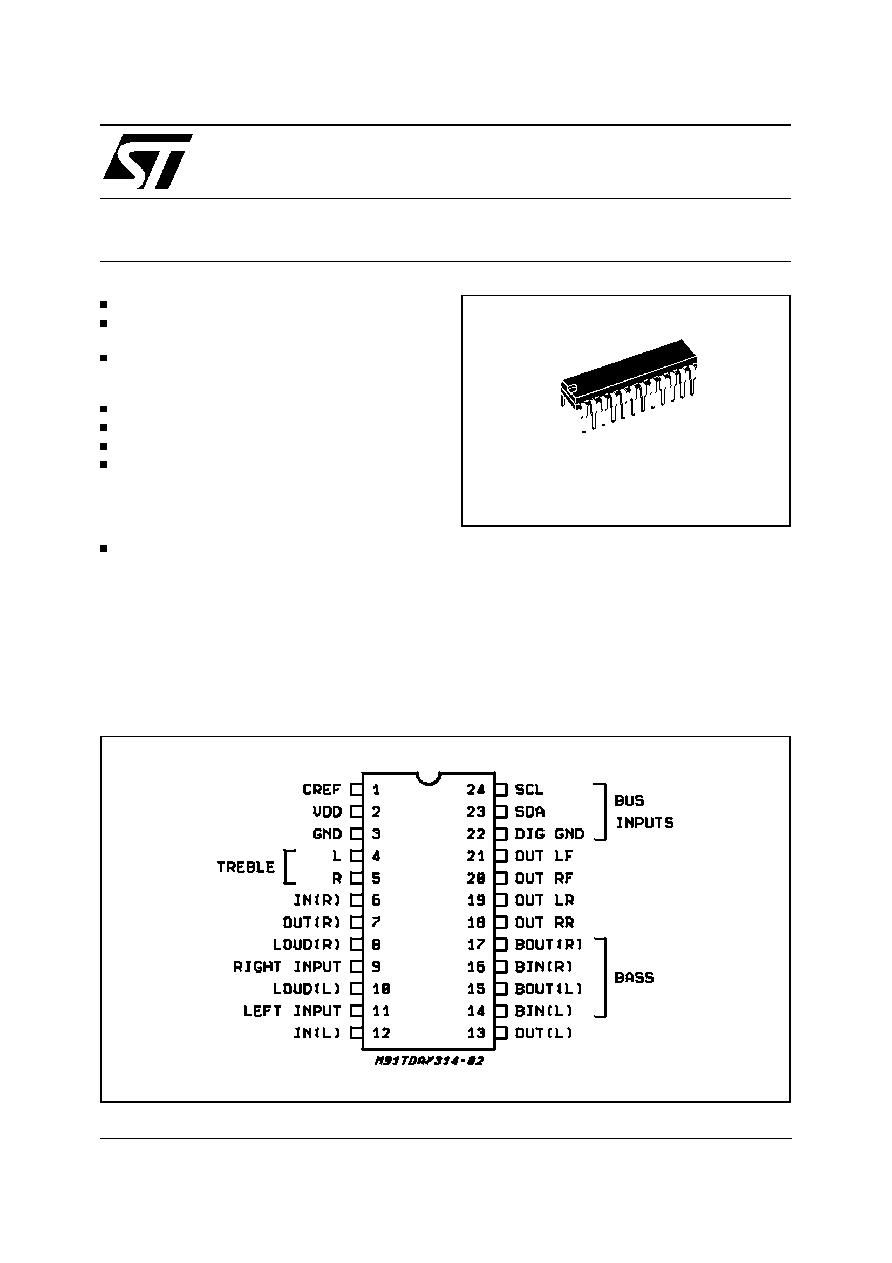
SDIP24
ORDERING NUMBER: TDA7314
PIN CONNECTION (Top view)
1/12

THERMAL DATA
Symbol
Description
Value
Unit
R
th j-pins
Thermal Resistance Junction-pins
Ma x.
65
∞
C/W
QUICK REFERENCE DATA
Symbol
Parameter
Min.
Typ.
Max.
Unit
V
S
Supply Voltage
6
9
10
V
V
CL
Max. input signal handling
2
Vrms
THD
Total Harmonic Distortion V = 1Vrms f = 1KHz
0.01
0.1
%
S/N
Signal to Noise Ratio
106
dB
S
C
Channel Separation f = 1KHz
103
dB
Volume Control
1.25dB step
-78.75
0
dB
Bass and Treble Control
2db step
-14
+14
dB
Fader and Balance Control
1.25dB step
-38.75
0
dB
Input Gain
6.25dB step
0
18.75
dB
Mute Attenuation
100
dB
ABSOLUTE MAXIMUM RATINGS
Symbol
Parameter
Value
Unit
V
S
Operating Supply Voltage
10.2
V
T
amb
Operating Ambient Temperature
-40 to 85
∞
C
T
stg
Storage Temperature Range
-55 to +150
∞
C
TEST CIRCUIT
TDA7314
2/12

BLOCK DIAGRAM
TDA7314
3/12

ELECTRICAL CHARACTERISTICS (refer to the test circuit T
amb
= 25
∞
C, V
S
= 9V, R
L
= 10K
, R
G
=
600
, all controls flat (G = 0), f = 1KHz unless otherwise specified)
Symbol
Parameter
Test Condition
Min.
Typ.
Max.
Unit
SUPPLY
V
S
Supply Voltage
6
9
10
V
I
S
Supply Current
8
11
mA
SVR
Ripple Rejection
60
80
dB
INPUT STAGE
R
II
Input Resistance
Pin 9, 11
35
50
70
K
V
CL
Clipping Level
2
2.5
Vrms
R
L
Output Load resistance
pin 7, 17
2
K
G
INmin
Min. Input Gain
-1
0
1
dB
G
INmax
Max. Input Gain
18.75
dB
G
STEP
Step Resolution
6.25
dB
e
IN
Input Noise
G = 18.75dB
2
µ
V
V
DC
DC Steps
adjacent gain steps
4
20
mV
G = 18.75 to Mute
4
mV
VOLUME CONTROL
R
IV
Input Resistance
20
33
50
k
C
RANGE
Control Range
70
75
80
dB
A
VMIN
Min. Attenuation
-1
0
1
dB
A
VMAX
Max. Attenuation
70
75
80
dB
A
STEP
Step Resolution
0.5
1.25
1.75
dB
E
A
Attenuation Set Error
Av = 0 to -20dB
Av = -20 to -60dB
-1.25
-3
0
1.25
2
dB
dB
E
T
Tracking Error
2
dB
V
DC
DC Steps
adjacent attenuation steps
From 0dB to Av max
0
0.5
3
7.5
mV
mV
SPEAKER ATTENUATORS
C
range
Control Range
35
37.5
40
dB
S
STEP
Step Resolution
0.5
1.25
1.75
dB
E
A
Attenuation set error
1.5
dB
A
MUTE
Output Mute Attenuation
80
100
dB
V
DC
DC Steps
adjacent att. steps
from 0 to mute
0
1
3
10
mV
mV
BASS CONTROL (1)
Gb
Control Range
Max. Boost/cut
+12
+14
+16
dB
B
STEP
Step Resolution
1
2
3
dB
R
B
Internal Feedback Resistance
34
44
58
K
TREBLE CONTROL (1)
Gt
Control Range
Max. Boost/cut
+13
+14
+15
dB
T
STEP
Step Resolution
1
2
3
dB
TDA7314
4/12

ELECTRICAL CHARACTERISTICS (continued)
Symbol
Parameter
Test Condition
Min.
Typ.
Max.
Unit
AUDIO OUTPUTS
V
OCL
Clipping Level
d = 0.3%
2
2.5
Vrms
R
L
Output Load Resistance
2
K
C
L
Output Load Capacitance
10
nF
R
OUT
Output resistance
30
75
120
V
OUT
DC Voltage Level
4.2
4.5
4.8
V
GENERAL
e
NO
Output Noise
BW = 20-20KHz, flat
output muted
all gains = 0dB
2.5
5
15
µ
V
µ
V
A curve all gains = 0dB
3
µ
V
S/N
Signal to Noise Ratio
all gains = 0dB; V
O
= 1Vrms
106
dB
d
Distortion
A
V
= 0, V
IN
= 1Vrms
A
V
= -20dB V
IN
= 1Vrms
V
IN
= 0.3Vrms
0.01
0.09
0.04
0.1
0.3
%
%
%
Sc
Channel Separation left/right
80
103
dB
Total Tracking error
A
V
= 0 to -20dB
-20 to -60 dB
0
0
1
2
dB
dB
BUS INPUTS
V
IL
Input Low Voltage
1
V
V
IH
Input High Voltage
3
V
I
IN
Input Current
-5
+5
µ
A
V
O
Output Voltage SDA
Acknowledge
I
O
= 1.6mA
0.4
V
Note:
(1) Bass and Treble response see attached diagram (fig.19). The center frequency and quality of the resonance behaviour can be choosen by
the external circuitry. A standard first order bass response can be realized by a standard feedback network.
Figure 1: Loudness versus Volume Attenuation
Figure 2: Loudnessversus Frequency
(C
LOUD
= 100nF)
TDA7314
5/12