 | –≠–ª–µ–∫—Ç—Ä–æ–Ω–Ω—ã–π –∫–æ–º–ø–æ–Ω–µ–Ω—Ç: 7403 | –°–∫–∞—á–∞—Ç—å:  PDF PDF  ZIP ZIP |
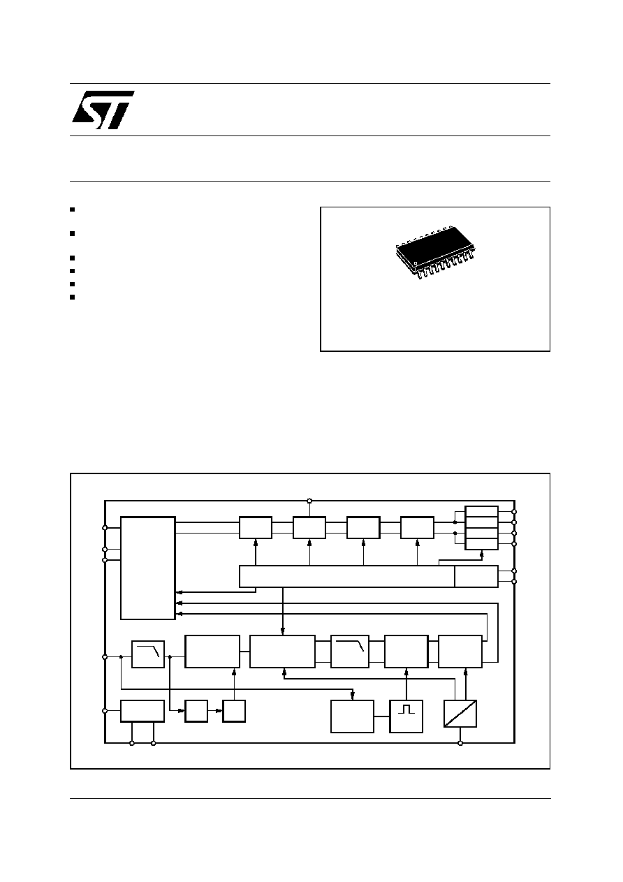
DEVICE INCLUDES AUDIO PROCESSOR,
STEREO DECODER AND NOISEBLANKER
HIGH PERFORMANCE SIGNAL PROCES-
SOR WITH BASIC FUNCTIONS
AM, FM, MPX AND CASSETTE INPUTS
NO EXTERNAL COMPONENTS REQUIRED
FULLY PROGRAMMABLE VIA I
2
C BUS
LOW DISTORTION AND NOISE
DESCRIPTION
The TDA7403 is a high performance signal proc-
essor specifically designed for car radio applica-
tions focused on the low-end market.
The device includes a complete audioprocessor
and a stereo decoder with noiseblanker.
Switched-capacitors design technique allows to
obtain all these features without external compo-
nents or adjustments. Using TDA7403 results is
in a very performant low-cost signal processing
application
The device is fully programmable by I
2
C bus in-
terface allowing to customize key device parame-
ters and especially filter characteristics.
The BICMOS process combined with the opti-
mized signal processing assure low noise and
low distortion performances.
This is preliminary information on a new product now in development or undergoing evaluation. Details are subject to change without notice.
October 1998
Æ
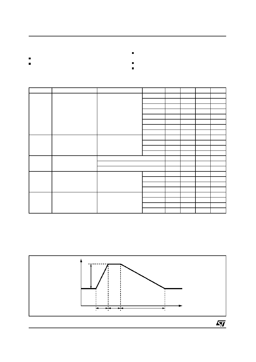
SUPPLY
DEMODULATOR
+ STEREO ADJUST
+ STEREO BLEND
CREF
OUT LR
D98AU918
DIGITAL CONTROL
PILOT
CANCELLATION
V
S
CASS L
INPUT
MULTIPLEXER
+
AUTO ZERO
MPX
VOLUME
BASS
TREBLE
OUT LR
OUT LF
OUT RR
OUT RF
OUT LF
OUT RR
OUT RF
SCL
SDA
80KHz
LP
FM R
FM L
PLL
25KHz
LP
S & H
HIGH
CUT
CONTROL
PULSE
FORMER
D
LEVEL
AM
CASS R
GND
SM
SOFT
MUTE
PIL
DET
I
2
C BUS
NOISE
BLANKER
A
8
1
2
9
15
14
20
11
17
19
16
18
12
13
10
BLOCK DIAGRAM
SO20
ORDERING NUMBER: TDA7403D
TDA7403
BASIC SIGNAL PROCESSOR
PRELIMINARY DATA
1/26

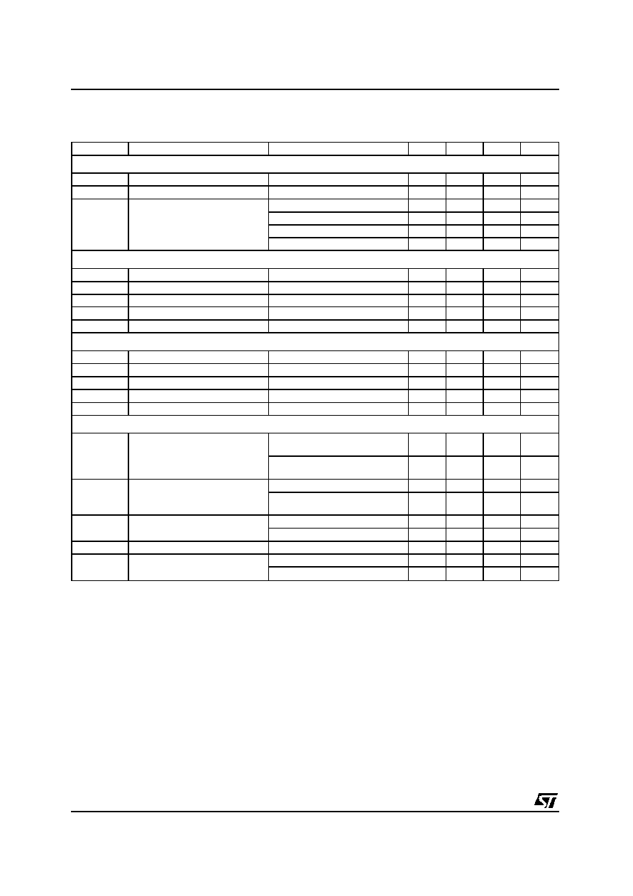
ABSOLUTE MAXIMUM RATINGS
Symbol
Parameter
Value
Unit
V
S
Operating Supply Voltage
10.5
V
T
amb
Operating Ambient Temperature Range
-40 to 80
∞
C
T
stg
Operating Storage Temperature Range
-55 to 150
∞
C
SUPPLY
Symbol
Parameter
Test Condition
Min.
Typ.
Max.
Unit
V
S
Supply Voltage
7.5
9
10
V
I
S
Supply Current
V
S
= 9V
25
30
35
mA
SVRR
Ripple Rejection @ 1KHz
Audioprocessor (all filters flat)
60
dB
Stereodecoder + Audioprocessor
55
dB
ESD
All pins are protected against ESD according to the MIL883 standard.
THERMAL DATA
Symbol
Parameter
Value
Unit
R
th-j pins
Thermal Resistance Junction-pins
Max
85
∞
C/W
CASS R
CASS L
N.C.
N.C.
N.C.
N.C.
N.C.
AM
MPX
SCL
SDA
GND
OUT RR
V
S
OUT LR
OUT RF
OUT LF
CREF
1
3
2
4
5
6
7
8
9
18
17
16
15
14
12
13
11
19
10
20
LEVEL
SM
D98AU919
PIN CONNECTION
TDA7403
2/26

PIN DESCRIPTION
N.
Name
Function
Type
1
CASSR
Cassette Input Right
I
2
CASSL
Cassette Input Left
I
3
n.c.
not connected
4
n.c.
not connected
5
n.c.
not connected
6
n.c.
not connected
7
n.c.
not connected
8
AM
AM Input
I
9
MPX
FM Input (MPX)
I
10
LEVEL
Level Input Stereodecoder
I
11
SM
Soft Mute Drive
I
12
SCL
I
2
C Clock Line
I/O
13
SDA
I
2
C Data Line
I/O
14
GND
Supply Ground
S
15
VS
Supply Voltage
S
16
OUTRR
Right Rear Speaker Output
O
17
OUTLR
Left Rear Speaker Output
O
18
OUTRF
Right Front Spaeaker Output
O
19
OUTLF
Left Front Speaker Output
O
20
CREF
Reference Capacitor Pin
S
(1) See input configuration tree and databyte specification "configuration"
Pin type legenda:
I = Input
O = Output
I/O = Input/Output
S = Supply
TDA7403
3/26

AUDIO PROCESSOR PART
Input Multiplexer
MPX input
Cassette stereo input
AM mono or stereo input
Internal beep with 2 frequencies (selectable)
Mixable phone and beep signals
Loudness
First or second order frequency response
Programmable center frequency and quality factor
15 x 1dB steps
Selectable flat-mode (constant attenuation)
Volume control
1dB attenuator
Max. gain 20dB
Max. attenuation 79dB
Soft-step gain control
Bass Control
2nd order frequency response
Center frequency programmable in 4(5) steps
DC gain programmable
7 x 2dB steps
Treble Control
2nd order frequency response
Center frequency programmable in 4 steps
7 x 2dB steps
Speaker Control
4 independent speaker controls (1dB steps
control range 50dB)
Mute Functions
Direct mute driven by pin SM
Digitally controlled softmute with 4 program-
mable time constants
ELECTRICAL CHARACTERISTICS (V
S
= 9V; T
amb
= 25
∞
C; R
L
= 10K
; all gains = 0dB; f = 1KHz;
unless otherwise specified).
Symbol
Parameter
Test Condition
Min.
Typ.
Max.
Unit
INPUT SELECTOR
R
in
Input Resistance
all inputs except Phone
70
100
130
K
V
CL
Clipping Level
2.2
2.6
V
RMS
S
IN
Input Separation
80
100
dB
G
IN MIN
Min. Input Gain
-1
0
1
dB
G
IN MAX
Max. Input Gain
14
dB
G
STEP
Step Resolution
2
dB
V
DC
DC Steps
Adjacent Gain Step
0
mV
G
MIN
to G
MAX
1
mV
BEEP CONTROL
V
RMS
Beep Level
350
mV
f
BMIN
Lower Beep Frequency
600
Hz
f
BMAX
Higher Beep Frequency
1.2
KHz
MIXING CONTROL
M
LEVEL
Mixing Level
Source
0
dB
Source
-6
dB
Source
-12
dB
Beep/Phone
0
dB
TDA7403
4/26

ELECTRICAL CHARACTERISTICS (continued)
Symbol
Parameter
Test Condition
Min.
Typ.
Max.
Unit
VOLUME CONTROL
G
MAX
Max Gain
20
dB
A
MAX
Max Attenuation
79
dB
A
STEP
Step Resolution
1
dB
E
A
Attenuation Set Error
G = -20 to 20dB
-1.25
0
1.25
dB
G = -60 to 20dB
-4
0
3
dB
E
T
Tracking Error
2
dB
V
DC
DC Steps
Adjacent Attenuation Steps
0.1
3
mV
From 0dB to G
MIN
0.5
5
mV
LOUDNESS CONTROL
A
STEP
Step Resolution
1
dB
A
MAX
Max. Attenuation
15
dB
f
CMIN
Lower Center Frequency
200
Hz
f
CMAX
Higher Center Frequency
400
Hz
SOFT MUTE
A
MUTE
Mute Attenuation
70
100
dB
T
D
Delay Time
T1
0.48
ms
T2
0.96
ms
T3
40.4
ms
T4
324
ms
V
THlow
Low Threshold for SM Pin
(1)
1
V
V
THhigh
High Threshold for SM Pin
2.5
V
R
PU
Internal Pull-up Resistor
70
100
130
K
V
PU
Pull-up Voltage
4.7
V
SOFT STEP
T
SW
Switch Time
10
ms
BASS CONTROL
C
RANGE
Control Range
±
14
dB
A
STEP
Step Resolution
2
dB
f
C
Center Frequency
f
C1
60
Hz
f
C2
70
Hz
f
C3
80
Hz
f
C4
100
(2)
Hz
Q
BASS
Quality Factor
Q
1
1
Q
2
1.25
Q
3
1.5
Q
4
2
DC
GAIN
Bass-Dc-Gain
DC = off
0
dB
DC = on
4.4
dB
1) SM pin is active low (mute condition)
2) See description of Audioprocessor Part - Bass & Treble filter characteristics programming
TDA7403
5/26
ELECTRICAL CHARACTERISTICS (continued)
Symbol
Parameter
Test Condition
Min.
Typ.
Max.
Unit
TREBLE CONTROL
C
RANGE
Control Range
±
14
dB
A
STEP
Step Resolution
2
dB
f
C
Center Frequency
f
C1
10
KHz
f
C2
12.5
KHz
f
C3
15
KHz
f
C4
17.5
KHz
SPEAKER ATTENUATORS
C
RANGE
Control Range
50
dB
A
STEP
Step Resolution
1
dB
A
MUTE
Output Mute Attenuation
80
90
dB
E
E
Attenuation Set Error
2
dB
V
DC
DC Steps
Adjacent Attenuation Steps
0.1
5
mV
AUDIO OUTPUTS
V
CLIP
Clipping Level
d = 0.3%
2.2
2.6
V
RMS
R
L
Output Load Resistance
2
K
C
L
Output Load Capacitance
10
nF
R
OUT
Output Impedance
30
120
V
DC
DC Voltage Level
3.8
V
GENERAL
e
NO
Output Noise
BW = 20 Hz to 20 KHz
output muted
3
µ
V
BW = 20 Hz to 20 KHz
all gain = 0dB
6.5
µ
V
S/N
Signal to Noise Ratio
all gain = 0dB flat; V
O
= 2V
RMS
110
dB
bass treble at 12dB; V
O
=
2.6V
RMS
100
dB
d
Distortion
V
IN
= 1V
RMS
; all stages 0dB
0.002
%
V
IN
= 1V
RMS
; Bass & Treble = 12dB
0.05
%
S
C
Channel separation Left/Right
80
100
dB
E
T
Total Tracking Error
A
V
= 0 to -20dB
0
1
dB
A
V
= -20 to -60dB
0
2
dB
TDA7403
6/26
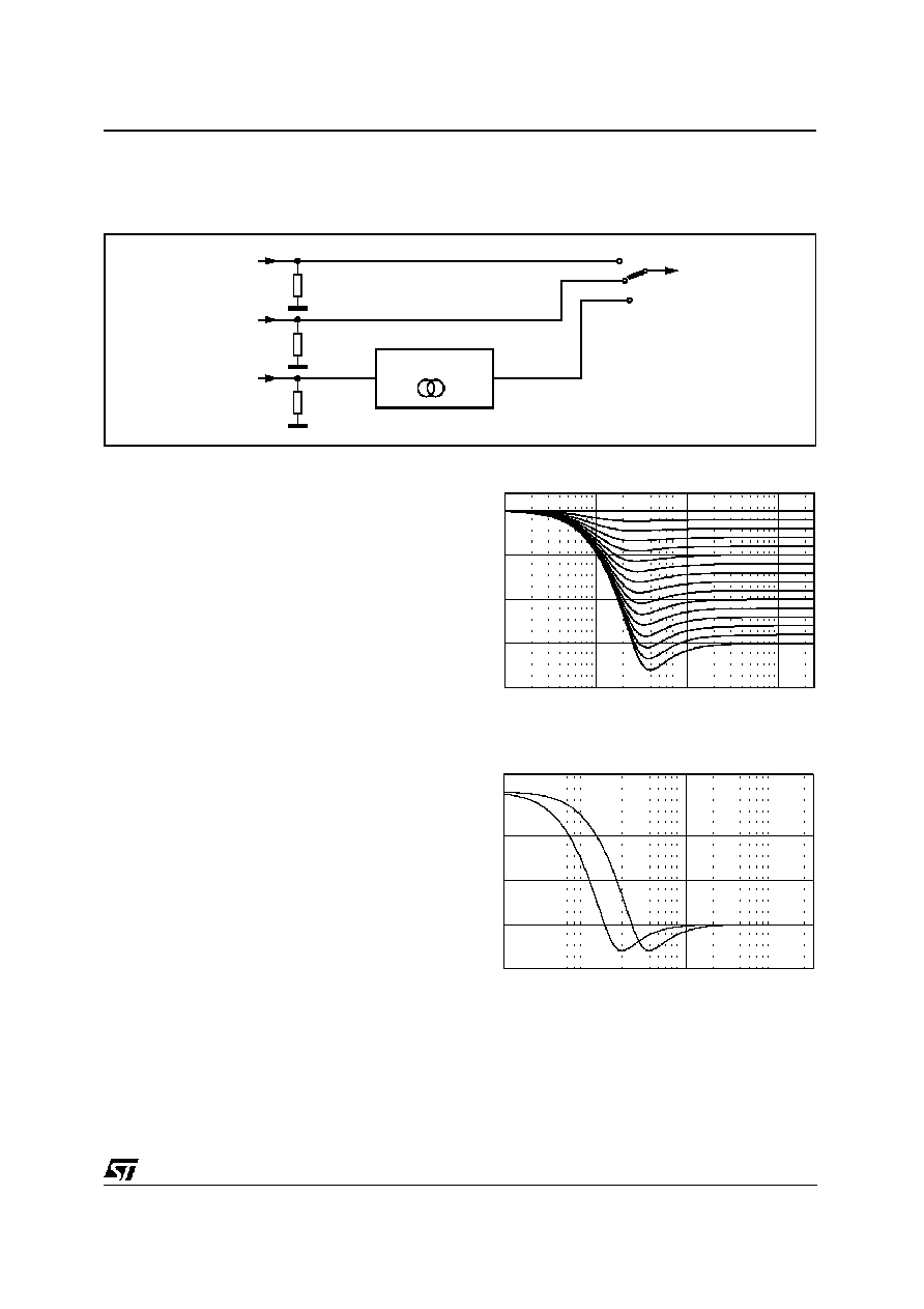
Input stages
The input circuits are the same as in preceeding
ST audioprocessors with exception of the CD in-
puts (see figure 1).
The typical input impedance is 100k
.
AutoZero
In order to reduce the number of pins there is no
AC coupling between the In-Gain and the follow-
ing stage, so that any offset generated by or be-
fore the In-Gain stage would be transferred or
even amplified to the output.
To avoid that effect a special offset cancellation
stage called AutoZero is implemented.
To avoid audible clicks the audioprocessor is
muted before the loudness stage during this time.
In some cases, for example if the
µ
P is executing
a refresh cycle of the I
2
C bus programming, it is
not useful to start a new AutoZero action because
no new source is selected and an undesired mute
would appear at the outputs. For such applica-
tions the TDA7403 could be switched in the "Auto
Zero Remain" mode (Bit 6 of the subaddress
byte). If this bit is set to high, the DATABYTE 0
could be loaded without invoking the AutoZero
and the old adjustment value remains.
Mixing Stage
This stage offers the possibility to mix the internal
beep or the phone signal to any other source.
Due to the fact that the mixing stage is also lo-
cated behind the In-Gain stage fine adjustments
of the main source level can be done in this way.
Loudness
There are four parameters programmable in the
loudness stage (see fig. 2, 3, 4):
- Attenuation
- Center Frequency
- Loudness Q
- Flat Mode: in this mode the loudness stage works
as a 0 - 15dB attenuator.
D98AU951
100K
100K
100K
STEREODECODER
IN GAIN
CASSETTE
AM
MPX
Figure 1. Input stages
-20.0
-15.0
-10.0
-5.0
0.0
10.0
100.0
1.0K
10.0K
Figure 2. Loudness Attenuation @ fc = 400Hz
(second order)
-20.0
-15.0
-10.0
-5.0
0.0
10.0
100.0
1.0K
10.0K
Figure 3. Loudness Center frequency @ Attn.
= 15dB (second order)
DESCRIPTION OF THE AUDIOPROCESSOR
TDA7403
7/26
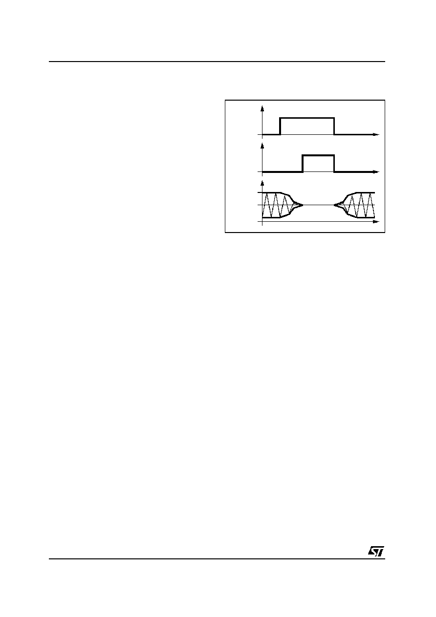
Softmute
The digitally controlled softmute stage allows
muting/demuting the signal with a I
2
C bus pro-
grammable slope. The mute process can either
be activated by the softmute pin or by the I
2
C
bus. The slope is realized in a special S shaped
curve to mute slow in the critical regions (see fig-
ure 5).
For timing purposes the Bit 3 of the I
2
C bus out-
put register is set to 1 from the start of muting un-
til the end of demuting.
Softstep Volume
When volume level is changed often an audible
click appears at the output. The root cause of
those clicks could be either a DC offset before
the volume stage or the sudden change of the
envelope of the audio signal. With the Softstep
feature both kinds of clicks could be reduced to a
minimum and are no more audible (see figure 6).
Bass
There are three parameters programmable in the
bass stage (see figs 7, 8, 9, 10):
- Attenuation
- Center Frequency (60, 70, 80 and 100Hz)
- Quality Factors (1, 1.25, 1.5 and 2)
DC Mode
In this mode the DC gain is increased by 4.4dB.
In addition the programmed center frequency and
quality factor is decreased by 25% which can be
used to reach alternative center frequencies or
quality factors.
Treble
There are two parameters programmable in the
treble stage (see figs 11, 12):
- Attenuation
- Center Frequency (10, 12.5, 15 and 17.5kHz).
Speaker Attenuator
Due to practical aspects the steps in the speaker
attenuators are not linear over the full range. At
attenuations more than 24dB the steps increase
from 1.5dB to 10dB (please see data byte specifi-
cation).
10
100
1,000
Hz
-20
-15
-10
-5
(dB)
D98AU844
Figure 4. Loudness @ Attn. = 15dB, fc = 400Hz
1
EXT.
MUTE
+SIGNAL
REF
-SIGNAL
1
I
2
C BUS
OUT
Time
D97AU634
Figure 5. Softmute Timing
2dB
1dB
-1dB
-2dB
Time
D97AU635
VOUT
10ms
Figure 6. Soft Step Timing
Note: Please notice that a started Mute action is always terminated
and could not be interrupted by a change of the mute signal.
Note: For steps more than 1dB the softstep mode should be
deactivated because it could generate a 1dB error during the
blend-time
TDA7403
8/26

0.0
2.5
5.0
7.5
10.0
12.5
15.0
10.0
100.0
1.0K
10.0K
Figure 10. Bass normal and DC Mode
@ Gain = 14dB, fc = 80Hz
0.0
2.5
5.0
7.5
10.0
12.5
15.0
10.0
100.0
1.0K
10.0K
Figure 9. Bass Quality factors @ Gain = 14dB,
fc = 80Hz
0.0
2.5
5.0
7.5
10.0
12.5
15.0
10.0
100.0
1.0K
10.0K
Figure 8. Bass Center @ Gain = 14dB, Q = 1
-15.0
-10.0
-5.0
0.0
5.0
10.0
15.0
10.0
100.0
1.0K
10.0K
Figure 7. Bass Control @ fc = 80Hz, Q = 1
0.0
2.5
5.0
7.5
10.0
12.5
15.0
10.0
100.0
1.0K
10.0K
Figure 12. Treble Center Frequencies
@ Gain = 14dB
-15.0
-10.0
-5.0
0.0
5.0
10.0
15.0
10.0
100.0
1.0K
10.0K
Figure 11. Treble Control @ fc = 17.5KHz
Note: In general the center frequency, Q and DC-mode can be set
independently. The exception from this rule is the mode (5/xx1111xx)
where the center frequency is set to 150Hz instead of 100Hz.
TDA7403
9/26

ELECTRICAL CHARACTERISTICS (V
S
= 9V; deemphasis time constant = 50
µ
s, V
MPX
= 500mV,
75KHz deviation, f = 1KHz. G
I
= 6dB, T
amb
= 25
∞
C; unless otherwise specified).
Symbol
Parameter
Test Condition
Min.
Typ.
Max.
Unit
V
IN
MPX Input Level
Input Gain = 3.5dB
0.5
1.25
V
RMS
R
in
Input Resistance
100
K
G
min
Minimum Input Gain
3.5
dB
G
max
Max Input Gain
11
dB
G
STEP
Step Resolution
2.5
dB
SVRR
Supply Voltage Ripple Rejection
V
ripple
= 100mv, f = 1khz
60
dB
Max Channel Separation
50
dB
THD
Total Harmonic Distortion
0.02
0.3
%
S
+
N
N
Signal plus Noise to Noise Ratio
S = 2V
rms
91
dB
MONO/STEREO SWITCH
V
PTHST1
Pilot Threshold Voltage
for Stereo, PTH = 1
15
mV
V
PTHST0
Pilot Threshold Voltage
for Stereo, PTH = 0
25
mV
V
PTHMO1
Pilot Threshold Voltage
for Mono, PTH = 1
12
mV
V
PTHMO0
Pilot Threshold Voltage
for Stereo, PTH = 0
19
mV
PLL
f/f
Capture Range
0.5
%
DEEMPHASIS and HIGHCUT
HC50
Deemphasis Time Constant
Bit = 7, Subadr. 10 = 0
V
LEVEL
>> V
HCH
50
µ
s
HC75
Deemphasis Time Constant
Bit = 7, Subadr. 10 = 1
VLEVEL >> V
HCH
75
µ
s
HC50
Highcut Time Constant
Bit = 7, Subadr. 10 = 0
VLEVEL >> V
HCL
150
µ
s
HC75
Highcut Time Constant
Bit = 7, Subadr. 10 = 1
VLEVEL >> V
HCL
225
µ
s
STEREOBLEND and HIGHCUT-CONTROL
REF5V
Internal Reference Voltage
5
V
TC
REF5V
Temperature Coefficient
3300
ppm
L
Gmin
Min. LEVEL Gain
0
dB
L
Gmax
Max. LEVEL Gain
10
dB
L
Gstep
LEVEL Gain Step Resolution
0.67
dB
VSBL
min
Min.Voltage for Mono
33
%REF5V
VSBL
max
Max. Voltage for Mono
58
%REF5V
VSBL
step
Step Resolution
8.4
%REF5V
STEREODECODER PART
No external components necessary
PLL with adjustment free fully integrated VCO
Automatic pilot dependent MONO/STEREO
switching
Very high suppression of intermodulation and
interference
Programmable Roll-Off compensation
Dedicated RDS Softmute
Highcut and Stereoblend characterisctics pro-
grammable in a wide range
Internal Noiseblanker with threshold controls
Multipath detector with programmable inter-
nal/external influence
I
2
C bus control of all necessary functions
TDA7403
10/26

ELECTRICAL CHARACTERISTICS (continued)
Symbol
Parameter
Test Condition
Min.
Typ.
Max.
Unit
STEREOBLEND and HIGHCUT CONTROL
VHCH
min
Min.Voltage for NO Highcut
42
%REF5V
VHCH
max
Max. Voltage for NO Highcut
66
%REF5V
VHCH
step
Step Resolution
8.4
%REF5V
VHCL
min
Min. Voltage for FULL High cut
17
%VHCH
VHCL
max
Max. Voltage for FULL High cut
33
%VHCH
Carrier and harmonic suppression at the output
19
Pilot Signal
f = 19KHz
50
dB
38
Subcarrier
f = 38KHz
75
dB
57
Subcarrier
f = 57KHz
62
dB
76
Subcarrier
f = 76KHz
90
dB
Intermodulation (Note1)
2
Pilot Signal
f
mod
= 10KHz; f
spur
= 1KHz;
65
dB
3
f
mod
= 13KHz; f
spur
= 1KHz;
75
dB
Traffic Radio (Note 2)
57
Signal
f = 57KHz
70
dB
SCA - Subsidiary Communications Authorization (Note 3)
67
Signal
f = 67KHz
75
dB
ACI - Adjacent Channel Interference (Note 4)
114
Signal
f = 114KHz
95
dB
190
Signal
f = 190KHz
84
dB
Notes to the characteristics:
1. Intermodulation Suppression: measured with: 91% pilot signal; fm = 10kHz or 13kHz.
2. Traffic Radio (V.F.) Suppression: measured with: 91% stereo signal; 9% pilot signal; fm=1kHz; 5% subcarrier (f = 57kHz,
fm = 23Hz AM, m = 60%)
3. SCA ( Subsidiary Communications Authorization ) measured with: 81% mono signal; 9% pilot signal; fm = 1kHz; 10%SCA - subcarrier
( fs = 67kHz, unmodulated ).
4. ACI ( Adjacent Channel Interference ) measured with: 90% mono signal; 9% pilot signal; fm =1kHz; 1% spurious signal
( fs = 110kHz or 186kHz, unmodulated).
TDA7403
11/26
ELECTRICAL CHARACTERISTICS (continued)
Symbol
Parameter
Test Condition
Min.
Typ.
Max.
Unit
V
TR
Trigger Threshold
0) 1)
meas. with V
PEAK
= 0.9V
NBT = 111
30
mV
OP
NBT = 110
35
mV
OP
NBT = 101
40
mV
OP
NBT = 100
45
mV
OP
NBT = 011
50
mV
OP
NBT = 010
55
mV
OP
NBT = 001
60
mV
OP
NBT = 000
65
mV
OP
V
TRNOISE
Noise Controlled Trigger
Threshold
2)
meas. with V
PEAK
= 1.5V
NCT = 00
260
mV
OP
NCT = 01
220
mV
OP
NCT = 10
180
mV
OP
NCT = 11
140
mV
OP
V
RECT
Rectifier Voltage
V
MPX
= 0mV
0.9
V
V
MPX
= 50mV; f = 150KHz
1.7
V
V
MPX
= 100mV; f = 150KHz
2.5
V
V
RECT DEV
deviation dependent
rectifier Voltage
3)
means. with
V
MPX
= 800mV
(75KHz dev.)
OVD = 11
0.9(off)
V
OP
OVD = 10
1.2
V
OP
OVD = 01
2.0
V
OP
OVD = 00
2.8
V
OP
V
RECT FS
Fieldstrength Controlled
Rectifier Voltage
4)
means. with
V
MPX
= 0mV
V
LEVEL
<< V
SBL
(fully mono)
FSC = 11
0.9(off)
V
FSC = 10
1.3
V
FSC = 01
1.8
V
FSC = 00
2.3
V
0) All thresholds are measured using a pulse with T
R
= 2
µ
s, T
HIGH
= 2
µ
s and T
F
= 10
µ
s.
1) NBT represents the Noiseblanker-Byte bits D2; D0 for the noise blanker trigger threshold
2) NAT represents the Noiseblanker-Byte bit pair D4,D3 for the noise controlled trigger adjustment
3) OVD represents the Noiseblanker-Byte bit pair D7,D6 for the over deviation detector
4) FSC represents the Fieldstrength-Byte bit pair D1,D0 for the fieldstrength control
VOP
VIN
DC
TR
THIGH
TF
Time
D97AU636
NOISE BLANKER PART
internal 2nd order 140kHz high pass filter
programmable trigger threshold
additional circuits for trigger adjustment (devia-
tion, field-strenght)
very low offset current during hold time
four selectable pulse suppression times
TDA7403
12/26

65mV
30mV
8 STEPS
NOISE CONTROLLED
TRIG. THRESHOLD
MIN. TRIG. THRESHOLD
260mV(00)
220mV(01)
180mV(10)
140mV(11)
0.9V
VTH
1.5V
VPEAK(V)
D97AU648
Figure 13. Trigger Threshold vs. V
PEAK
VPEAK
(V
OP
)
D97AU649
20
DEVIATION(KHz)
0.9
1.2
2.0
2.8
DETECTOR OFF (11)
32.5
45
75
10
01
00
Figure 14. Deviation Controlled Trigger
Adjustment
2.3V(00)
0.9V
VPEAK
E'
D98AU863
1.8V(01)
1.3V(10)
MONO
STEREO
noisy signal
good signal
ATC_SB OFF (11)
NOISE
ª3V
Figure 15. Fieldstrength Controlled Trigger
Adjustment
INGAIN
3.5 ... 11dB
STEP 2.5dB
INFILTER
LP 80KHz
4.th ORDER
DEMODULATOR
- PLOT CANC
- ROLL-OFF COMP.
- LP 25KHz
PLL +
PILOT-DET.
F19
NOISE BLANKER
F38
STEREO
HOLDN
SB CONTROL
DEEMPHASIS
+ HIGHCUT
t=50 or 75
µ
s
REF 5V
VSBL
LEVEL INTERN
HC
CONTROL
VHCCH
VHCCL
D
A
LEVEL INPUT
LP 2.2KHZ
1.th ORDER
LEVEL
FM_L
FM_R
MPX
100K
D98AU952
GAIN 0..10dB
Figure 16. Block diagram of the stereo decoder
TDA7403
13/26
DESCRIPTION OF STEREODECODER
The stereodecoder part of the TDA7403 (see Fig.
16) contains all functions necessary to demodu-
late the MPX signal like pilot tone dependent
MONO/STEREO
switching
as
well
as
"stereoblend" and "highcut" functions.
Adaptations like programmable input gain, roll-off
compensation, selectable deemphasis time con-
stant and a programmable fieldstrength input al-
low to use different IF devices.
Stereodecoder Mute
The TDA7403 has a fast and easy to control RDS
mute function which is a combination of the
audioprocessor softmute and the high-ohmic
mute of the stereodecoder. If the stereodecoder
is selected and a softmute command is sent (or
activated through the SM pin) the stereodecoder
will be set automatically to the high-ohmic mute
condition after the audio signal has been soft-
muted.
Hence a checking of alternate frequencies could
be performed. To release the system from the
mute condition simply the unmute command must
be sent: the stereodecoder is unmuted immedi-
ately and the audioprocessor is softly unmuted.
Fig. 17 shows the output signal V
O
as well as the
internal stereodecoder mute signal. This influ-
ence of Softmute on the stereodecoder mute can
be switched off by setting bit 3 of the Softmute
byte to "0". A stereodecoder mute command (bit
0, stereodecoder byte set to "1") will set the
stereodecoder in any case independently to the
high-ohmic mute state.
If any other source than the stereodecoder is se-
lected the decoder remains muted and the MPX
pin is connected to Vref to avoid any discharge of
the coupling capacitor through leakage currents.
Input Stages
The Ingain stage allows to adjust the MPX signal
to a magnitude of about 1Vrms internally which is
the recommended value. The 4.th order input fil-
ter has a corner frequency of 80kHz and is used
to attenuate spikes and noise and acts as an anti-
aliasing filter for the following switch capacitor fil-
ters.
Demodulator
In the demodulator block the left and the right
channel are separated from the MPX signal. In
this stage also the 19 kHz pilot tone is cancelled.
For reaching a high channel separation the
TDA7403 offers an I2C bus programmable roll-off
adjustment which is able to compensate the low-
pass behaviour of the tuner section. If the tuner
attenuation at 38kHz is in a range from 20.2% to
31% the TDA7403 needs no external network be-
fore the MPX pin. Within this range an adjustment
to obtain at least 40dB channel separation is pos-
sible.
The bits for this adjustment are located together
with the fieldstrength adjustment in one byte. This
gives the possibility to perform an optimization
step during the production of the carradio where
the channel separation and the fieldstrength con-
trol are trimmed.
Deemphasis and Highcut
The lowpass filter for the deemphasis allows to
choose between a time constant of 50
µ
s and
75
µ
s (bit D7, Stereodecoder byte).
The highcut control range will be in both cases
t
HC
= 2
t
Deemp
. Inside the highcut control range
(between VHCH and VHCL) the LEVEL signal
is converted into a 5 bit word which controls the
lowpass time constant between t
Deemp
...3
t
Deemp
.
There by the resolution will remain always 5 bits
independently of the absolute voltage range be-
tween the VHCH and VHCL values.
The highcut function can be switched off by I2C
bus (bit D7, Fieldstrength byte set to "0").
PLL and Pilot Tone Detector
The PLL has the task to lock on the 19kHz pilo-
tone during a stereo transmission to allow a cor-
rect demodulation. The included detector enables
the demodulation if the pilot tone reaches the se-
lected pilottone threshold VPTHST. Two different
thresholds are available. The detector output (sig-
nal STEREO, see block diagram) can be checked
SOFTMUTE
COMMAND
STD MUTE
V
O
t
D97AU638
t
t
Figure 17. Signals during stereodecoder's
softmute
TDA7403
14/26

by reading the status byte of the TDA7403 via
I2C bus.
Fieldstrength Control
The fieldstrength input is used to control the high
cut and the stereoblend function. In addition the
signal can be also used to control the noise-
blanker thresholds.
LEVEL Input and Gain
To suppress undesired high frequency modula-
tion on the highcut and stereoblend function the
LEVEL signal is lowpass filtered firstly. The filter
is a combination of a 1st order RC lowpass at
53kHz (working as anti-aliasing filter) and a 1st-
order switched capacitor lowpass at 2.2kHz. The
second stage is a programmable gain stage to
adapt the LEVEL signal internally to different IF.
The gain is widely programmable in 16 steps
from 0dB to 10dB (step = 0.67dB). These 4 bits
are located together with the Roll-Off bits in the
"Stereodecoder Adjustment" byte to simplify a
possible adaptation during the production of the
carradio.
Stereoblend Control
The stereoblend control block converts the inter-
nal LEVEL voltage (LEVEL INTERN) into an de-
modulator compatible analog signal which is used
to control the channel separation between 0dB
and the maximum separation. Internally this con-
trol range has a fixed upper limit which is the in-
ternal reference voltage REF5V. The lower limit
can be programmed to be 33%, 42%, 50% or
58% of REF5V (see fig. 19).
To adjust the external LEVEL voltage to the inter-
nal range two values must be defined: the LEVEL
gain L
G
and VSBL. To adjust the voltage where
the full channel separation is reached (VST) the
LEVEL gain L
G
has to be defined. The following
equation can be used to estimate the gain:
L
G
=
REF5V
Field strength voltage
[STEREO]
The gain can be programmed through 4 bits in
the "Stereodecoder-Adjustment" byte.
The MONO voltage VMO (0dB channel separa-
tion) can be choosen selecting 33, 42, 50 or 58%
of REF5V.
All necessary internal reference voltages like
REF5V are derived from a bandgap circuit.
Therefore they have a temperature coefficient
near zero. This is useful if the fieldstrength signal
is also temperature compensated.
But most IF devices apply a LEVEL voltage with a
TC of 3300ppm. The TDA7403 offers this TC for
the reference voltages, too. The TC is selectable
with bit D7 of the "stereodecoder adjustment"
byte.
Figure 18. Internal stereoblend characteristics
INTERNAL
VOLTAGES
t
D97AU639
VSBL
REF 5V
SETUP OF VST
INTERNAL
VOLTAGES
t
33%
REF 5V
SETUP OF VMO
LEVEL
LEVEL INTERN
FIELDSTRENGHT VOLTAGE
VST
VMO
LEVEL INTERN
42%
50%
58%
VSBL
VST
VMO
FIELDSTRENGHT VOLTAGE
Figure 19. Relation between internal and external LEVEL voltage and setup of Stereoblend
TDA7403
15/26
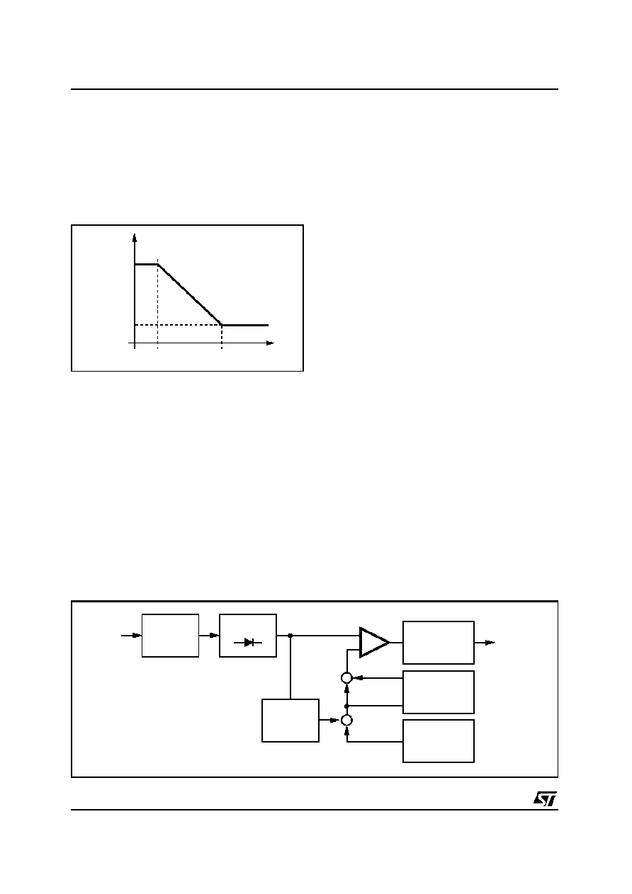
Highcut Control
The highcut control setup is similar to the
stereoblend control setup : the starting point
VHCH can be set with 2 bits to be 42, 50, 58 or
66% of REF5V whereas the range can be set to
be 17 or 33% of VHCH (see fig. 20).
FUNCTIONAL DESCRIPTION OF THE NOISE-
BLANKER
In the automotive environment the MPX signal is
disturbed by spikes produced by the ignition and
for example the wiper motor. The aim of the
noiseblanker part is to cancel the audible influ-
ence of the spikes. Therefore the output of the
stereodecoder is held at the actual voltage for
40
µ
s.
In a first stage the spikes must be detected but to
avoid a wrong triggering on high frequency
(white) noise a complex trigger control is imple-
mented. Behind the triggerstage a pulse former
generates the "blanking" pulse. To avoid any
crosstalk to the signalpath the noiseblanker is
supplied by his own biasing circuit.
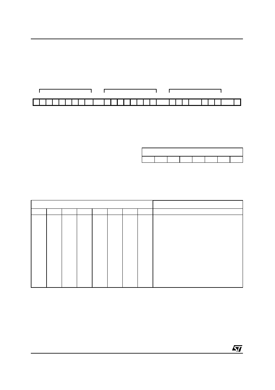
Trigger Path
The incoming MPX signal is highpass filtered,
amplified and rectified. This second order high-
pass-filter has a corner frequency of 140kHz. The
rectified signal, RECT, is lowpass filtered to gen-
erate a signal called PEAK. Also noise with a fre-
quency 140kHz increases the PEAK voltage. The
PEAK voltage is fed to a threshold generator,
which adds to the PEAK voltage a DC depend-
ent threshold VTH. Both signals, RECT and
PEAK+VTH are fed to a comparator which trig-
gers a re-triggerable monoflop. The monoflop's
output activates the sample-and-hold circuits in
the signalpath for 40
µ
s.
The block diagram of the noiseblanker is given in
fig.20.
Automatic Noise Controlled Threshold Adjust-
ment (ATC)
There are mainly two independent possibilities for
programming the trigger threshold:
a the low threshold in 8 steps (bits D0 to D2 of
the noiseblanker byte)
b the noise adjusted threshold in 4 steps
(bits D3 and D4 of the noiseblanker byte,
see fig. 13).
The low threshold is active in combination with a
good MPX signal without any noise; the PEAK
voltage is less than 1V. The sensitivity in this op-
eration is high.
If the MPX signal is noisy the PEAK voltage in-
creases due to the higher noise, which is also
rectified. With increasing of the PEAK voltage the
trigger threshold increases, too.
This particular
gain is programmable in 4 steps (see fig. 13).
LOWPASS
TIME CONSTANT
D97AU640
Deemp
FIELDSTRENGHT
VHCH
VHCL
3
∑
Deemp
Figure 20. Highcut characteristics
+
-
RECTIFIER
LOWPASS
RECT
+
+
THRESHOLD
GENERATOR
VTH
PEAK
ADDITIONAL
THRESHOLD
CONTROL
MONOFLOP
HOLDN
MPX
D98AU861
HIGH PASS
Figure 21. Block diagram of the noiseblanker
TDA7403
16/26

Automatic Threshold Control
Besides the noise controlled threshold adjust-
ment there is an additional possibility for influenc-
ing the trigger threshold. It is depending on the
stereoblend control.
The point where the MPX signal starts to become
noisy is fixed by the RF part. Therefore also the
starting point of the normal noise-controlled trig-
ger adjustment is fixed (fig. 15). In some cases
the behaviour of the noiseblanker can be im-
proved by increasing the threshold even in a re-
gion of higher fieldstrength. Sometimes a wrong
triggering occures for the MPX signal often shows
distortion in this range which can be avoided
even if using a low threshold.
Because of the overlap of this range and the
range of the stereo/mono transition it can be con-
trolled by stereoblend. This threshold increase is
programmable in 3 steps or switched off with bits
D0 and D1 of the fieldstrength control byte.
Over Deviation Detector
If the system is tuned to stations with a high de-
viation the noiseblanker can trigger on the higher
frequencies of the modulation. To avoid this
wrong behaviour, which causes noise in the out-
put signal, the noiseblanker offers a deviation de-
pendent threshold adjustment.
By rectifying the MPX signal a further signal rep-
resenting the actual deviation is obtained. It is
used to increase the PEAK voltage. Offset and
gain of this circuit are programmable in 3 steps
with the bits D6 and D7 of the stereodecoder byte
(the first step turns off the detector, see fig. 15).
TEST MODE
During the test mode which can be activated by
setting bit D0 of the testing byte and bit D5 of the
subaddress byte to "1" several internal signals
are available at the CASSR pin.
During this
mode the input resistance of 100kOhm is discon-
nected from the pin. The internal signals available
are shown in the software specification.
=
+V
CC
9V
100nF
CASS R
CASS L
100nF
100nF
CASS R
CASS L
OUTRR
OUTRR
OUTLR
OUTLR
OUTRF
OUTRF
OUTLF
OUTLF
CREF
10
µ
F
D98AUxx5
LEVEL
SMUTE
SCL
SDA
LEVEL
SMUTE
SCL
SDA
GND
V
S
MPX
220nF
MPX
AM
220nF
AM
Figure 23. Application Example.
TDA7403
17/26
I
2
C BUS INTERFACE DESCRIPTION
Interface Protocol
The interface protocol comprises:
-a start condition (S)
-a chip address byte (the LSB bit determines read
/ write transmission)
-a subaddress byte
-a sequence of data (N-bytes + acknowledge)
-a stop condition (P)
D97AU627
S
1
0
0
0
1
1
0 R/W ACK
ACK
ACK
P
MSB
LSB
MSB
LSB
MSB
LSB
CHIP ADDRESS
X
I
SUBADDRESS
DATA 1 to DATA n
AZ T
A3 A2 A1 A0
DATA
S = Start
ACK = Acknowledge
AZ = AutoZero-Remain
T = Testing
I = Autoincrement
P = Stop
MAX CLOCK SPEED 500kbits/s
The transmitted data is automatically updated af-
ter each ACK.
Transmission can be repeated without new chip
address.
Auto increment
If bit I in the subaddress byte is set to "1", the
autoincrement of the subaddress is enabled.
TRANSMITTED DATA (send mode)
MSB
LSB
X
X
X
X
ST
SM
X
X
SM = Soft mute activated
ST = Stereo
X = Not Used
SUBADDRESS (receive mode)
MSB
LSB
FUNCTION
X
AZ
T
I
A3
A2
A1
A0
0
0
0
0
0
0
0
0
1
1
1
1
1
1
1
1
0
0
0
0
1
1
1
1
0
0
0
0
1
1
1
1
0
0
1
1
0
0
1
1
0
0
1
1
0
0
1
1
0
1
0
1
0
1
0
1
0
1
0
1
0
1
0
1
Not allowed
Loudness / Auto-Zero
Volume
Softmute / Beep
Bass / Treble Attenuator
Bass / Treble Configuration
Speaker attenuator LF
Speaker attenuator LR
Speaker attenuator RF
Speaker attenuator RR / Blanktime adjust
Stereodecoder
Noiseblanker
Fieldstrength Control
Configuration
Stereodecoder Adjustment
Testing
T = Testmode
I = Autoincrement
AZ = Auto Zero Remain
X = not used
TDA7403
18/26

DATA BYTE SPECIFICATION
Input Selector
MSB
LSB
FUNCTION
D7
D6
D5
D4
D3
D2
D1
D0
0
0
0
0
1
1
1
1
0
0
1
1
0
0
1
1
0
1
0
1
0
1
0
1
Source Selector
don't use
Cassette
don't use
AM
Stereo Decoder
Input FM
Mute
don't use
0
1
CD Mode
CD Full-differential
CD Quasi-diff
1
0
0
1
0
0
1
1
1
1
0
0
1
1
0
0
AM/FM Mode
AM mono
AM stereo
AM through Stereo/Decoder
FM- Stereo/Decoder
0
0
:
1
1
0
0
:
1
1
0
1
:
0
1
In-Gain
14dB
12dB
:
2 dB
0 dB
For example to select the CD input in quasi-differential mode with gain of 8dB the Data Byte is: 0/0 1111000
Loudness
MSB
LSB
LOUDNESS
D7
D6
D5
D4
D3
D2
D1
D0
0
0
:
1
1
0
0
:
1
1
0
0
:
1
1
0
1
:
0
1
Attenuation
0dB
-1dB
:
-14dB
-15dB
0
1
Filter
on
off (flat)
0
1
Center Frequency
200Hz
400Hz
0
1
Loud ness Q
low (1
st
order)
normal (2
nd
order)
1
must be "1"
Note: The attenuation is specified at high frequencies. Around the center frequency the value is different depending on the programmed
attenuation (see Loudness frequency response).
TDA7403
19/26

Mute, Beep and Mixing
MSB
LSB
MUTE/BEEP/MIXING
D7
D6
D5
D4
D3
D2
D1
D0
0
1
0
0
1
1
0
1
0
1
0
1
Mute
Enable Softmute
Disable Softmute
Mute time =0.48 ms
Mute time =0.96 ms
Mute time =40.4 ms
Mute time =324 ms
Stereo Decoder Softmute Influence = off
Stereo Decoder Softmute Influence = on
0
1
Beep
Beep Frequency = 600Hz
Beep Frequency = 1.2KHz
0
0
1
1
0
1
0
1
0
1
Mixing
Mix-Source = Beep
Mix-Source = Phone
Full Mix Signal
Source -12dB + Mix-Signal -2.5dB
Source -6dB + Mix-Signal -6dB
Full Source
Note: for more information to the Stereodecoder-Softmute-Influence please refer to the stereodecoder description.
Volume
MSB
LSB
ATTENUATION
D7
D6
D5
D4
D3
D2
D1
D0
0
0
:
0
0
0
:
0
0
0
:
1
1
0
0
:
0
0
0
:
0
1
1
:
1
1
0
0
:
0
0
0
:
1
0
0
:
0
0
0
0
:
1
1
1
:
1
0
0
:
1
1
0
0
:
1
1
1
:
1
0
0
:
1
1
0
0
:
0
0
1
:
1
0
0
:
1
1
0
1
:
0
1
0
:
1
0
1
:
0
1
Gain/Attenuation
+32dB
+31dB
:
+20dB
+19dB
+18dB
:
+1dB
0dB
- 1dB
:
-78dB
-79dB
0
1
Softstep
Softstep Volume = off
Softstep Volume = on
Note: It is not recommended to use a gain more than 20dB for system performance reason. In general, the max. gain should be limited by
software to the maximum value, which is needed for the system.
TDA7403
20/26

Bass & Treble Attenuation
MSB
LSB
BASS & TREBLE ATTENUATION
D7
D6
D5
D4
D3
D2
D1
D0
0
0
:
0
0
1
1
:
1
1
0
0
:
1
1
1
1
:
0
0
0
0
:
1
1
1
1
:
0
0
0
1
:
0
1
1
0
:
1
0
Treble Steps
-14dB
-12dB
:
-2dB
0dB
0dB
+2dB
:
+12dB
+14dB
0
0
:
0
0
1
1
:
1
1
0
0
:
1
1
1
1
:
0
0
0
0
:
1
1
1
1
:
0
0
0
1
:
0
1
1
0
:
1
0
Bass Steps
-14dB
-12dB
:
-2dB
0dB
0dB
+2dB
:
+12dB
+14dB
For example 12dB Treble and -8dB Bass give the following DATA BYTE : 0 0 1 1 1 0 0 1.
Bass & Treble Filter Characteristics
MSB
LSB
BASS & TREBLE FILTER
D7
D6
D5
D4
D3
D2
D1
D0
0
0
1
1
0
1
0
1
Treble
Center Frequency = 10 KHz
Center Frequency = 12.5 KHz
Center Frequency = 15 KHz
Center Frequency = 17.5 KHz
0
1
1
0
0
1
1
1
0
1
0
1
0
0
1
1
1
0
1
0
1
1
Bass
Center Frequency = 60 Hz
Center Frequency = 70 Hz
Center Frequency = 80 Hz
Center Frequency = 100Hz
Center Frequency = 150Hz
Quality factor = 1
Quality factor = 1.25
Quality factor = 1.5
Quality factor = 2
DC-Gain = 0dB
DC-Gain =
±
4.4dB
1
must be "1"
For example Treble center frequency = 15kHz, Bass center frequency = 100Hz, Bass Q = 1 and DC = 0dB give the following DATA BYTE: 1
0 0 0 1 1 1 0
TDA7403
21/26
Speaker Attenuation (LF, LR, RF, RR)
MSB
LSB
D7
D6
D5
D4
D3
D2
D1
D0
1
1
0
0
:
0
0
0
0
0
0
0
0
0
1
0
0
:
1
1
1
1
1
1
1
1
1
0
0
:
0
1
1
1
1
1
1
1
1
0
0
:
1
0
0
0
0
1
1
1
1
0
0
:
1
0
0
1
1
0
0
1
1
0
1
:
1
0
1
0
1
0
1
0
1
Attenuation
0dB
-1dB
:
-23dB
-24.5dB
-26dB
-28dB
-30
-32dB
-35dB
-40dB
-50dB
Speaker Mute
Must be "1" (except RR speaker; see below)
0
0
1
1
0
1
0
1
Blank Time adj. (only at RR speaker)
38
µ
s
25.5
µ
s
32
µ
s
22
µ
s
Stereodecoder
MSB
LSB
FUNCTION
D7
D6
D5
D4
D3
D2
D1
D0
0
1
STD Unmuted
STD Muted
0
0
1
1
0
1
0
1
IN-Gain 11dB
IN-Gain 8.5dB
IN-Gain 6dB
IN-Gain 3.5dB
1
must be "1"
1
1
0
1
Forced MONO
MONO/STEREO switch automatically
0
1
Pilot Threshold HIGH
Pilot Threshold LOW
0
1
Deemphasis 50
µ
s
Deemphasis 75
µ
s
TDA7403
22/26
Noiseblanker
MSB
LSB
FUNCTION
D7
D6
D5
D4
D3
D2
D1
D0
0
0
0
0
1
1
1
1
0
0
1
1
0
0
1
1
0
1
0
1
0
1
0
1
Low Threshold 65mV
Low Threshold 60mV
Low Threshold 55mV
Low Threshold 50mV
Low Threshold 45mV
Low Threshold 40mV
Low Threshold 35mV
Low Threshold 30mV
0
0
1
1
0
1
0
1
Noise Controlled Threshold 320mV
Noise Controlled Threshold 260mV
Noise Controlled Threshold 200mV
Noise Controlled Threshold 140mV
0
1
Noise blanker OFF
Noise blanker ON
0
0
1
1
0
1
0
1
Over deviation Adjust 2.8V
Over deviation Adjust 2.0V
Over deviation Adjust 1.2V
Over deviation Detector OFF
Fieldstrength Control
MSB
LSB
FUNCTION
D7
D6
D5
D4
D3
D2
D1
D0
0
0
1
1
0
1
0
1
Noiseblanker Field strength Adj 2.3V
Noiseblanker Field strength Adj 1.8V
Noiseblanker Field strength Adj 1.3V
Noiseblanker Field strength Adj OFF
0
0
1
1
0
1
0
1
VSBL at 33% REF 5V
VSBL at 42% REF 5V
VSBL at 50% REF 5V
VSBL at 58% REF 5V
0
0
1
1
0
1
0
1
VHCH at 42% REF 5V
VHCH at 50% REF 5V
VHCH at 58% REF 5V
VHCH at 66% REF 5V
1
0
VHCL at 17% VHCH
VHCL at 33% VHCH
0
1
High cut OFF
High cut ON
TDA7403
23/26

Stereodecoder Adjustment
MSB
LSB
FUNCTION
D7
D6
D5
D4
D3
D2
D1
D0
0
0
0
:
1
:
1
0
0
1
:
0
:
1
0
1
0
:
0
:
1
Roll-Off Compensation
not allowed
20.2%
21.9%
:
25.5%
:
31.0%
0
0
0
:
1
0
0
0
:
1
0
0
1
:
1
0
1
0
:
1
LEVEL Gain
0dB
0.66dB
1.33dB
:
10dB
0
1
Temperature compensation at LEVEL inpu t
TC = 0
TC = 16.7mV/K (3300ppm)
Testing
MSB
LSB
FUNCTION
D7
D6
D5
D4
D3
D2
D1
D0
0
1
Stereodecoder test signals
OFF
Test signals enabled if bit D5 of the subaddress
(test mode bit) is set to "1", too
0
1
External Clock
Internal Clock
0
0
0
0
0
0
0
0
1
1
1
1
1
1
1
1
0
0
0
0
1
1
1
1
0
0
0
0
1
1
1
1
0
0
1
1
0
0
1
1
0
0
1
1
0
0
1
1
0
1
0
1
0
1
0
1
0
1
0
1
0
1
0
1
Testsignals at CASS_R
VHCCH
Level intern
Pilot magnitude
VCOCON; VCO Control Voltage
Pilot threshold
HOLDN
NB threshold
F228
VHCCL
VSBL
not used
not used
PEAK
not used
REF5V
not used
0
1
VCO
OFF
ON
0
1
Audio processor test mode
only if bit D5 of the subaddress
(test mode bit) is set to "1"
OFF
Note : This byte is used fortesting or evaluation purposes only and must not be set to other values than the default "11111110" in the application!
TDA7403
24/26
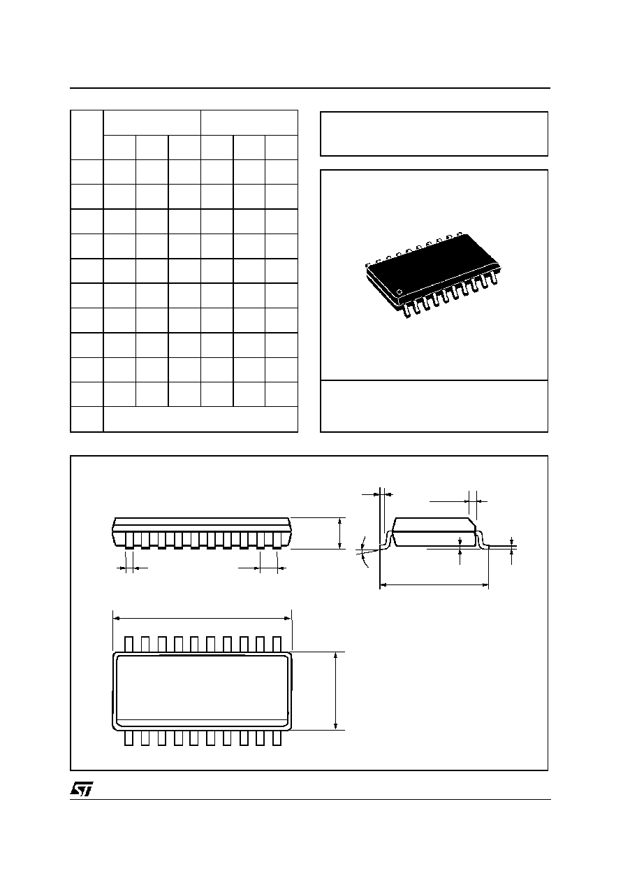
1
1
0
11
20
A
e
B
D
E
L
K
H
A1
C
SO20MEC
h x 45
∞
SO20
DIM.
mm
inch
MIN.
TYP.
MAX.
MIN.
TYP.
MAX.
A
2.35
2.65
0.093
0.104
A1
0.1
0.3
0.004
0.012
B
0.33
0.51
0.013
0.020
C
0.23
0.32
0.009
0.013
D
12.6
13
0.496
0.512
E
7.4
7.6
0.291
0.299
e
1.27
0.050
H
10
10.65
0.394
0.419
h
0.25
0.75
0.010
0.030
L
0.4
1.27
0.016
0.050
K
0
∞
(min.)8
∞
(max.)
OUTLINE AND
MECHANICAL DATA
TDA7403
25/26

Information furnished is believed to be accurate and reliable. However, STMicroelectronics assumes no responsibility for the consequences
of use of such information nor for any infringement of patents or other rights of third parties which may result from its use. No license is
granted by implication or otherwise under any patent or patent rights of STMicroelectronics. Specification mentioned in this publication are
subject to change without notice. This publication supersedes and replaces all information previously supplied. STMicroelectronics products
are not authorized for use as critical components in life support devices or systems without express written approval of STMicroelectronics.
The ST logo is a registered trademark of STMicroelectronics
©
1999 STMicroelectronics ≠ Printed in Italy ≠ All Rights Reserved
STMicroelectronics GROUP OF COMPANIES
Australia - Brazil - Canada - China - France - Germany - Italy - Japan - Korea - Malaysia - Malta - Mexico - Morocco - The Netherlands -
Singapore - Spain - Sweden - Switzerland - Taiwan - Thailand - United Kingdom - U.S.A.
http://www.st.com
TDA7403
26/26