M54/M74HC192
M54/M74HC193
October 1992
HC193 - SYNCHRONOUS UP/DOWN BINARY COUNTER
HC192 - SYNCHRONOUS UP/DOWN DECADE COUNTER
B1R
(Plastic Package)
ORDER CODES :
M54HCXXXF1R
M74HCXXXM1R
M74HCXXXB1R
M74HCXXXC1R
F1R
(Ceramic Package)
M1R
(Micro Package)
C1R
(Chip Carrier)
PIN CONNECTIONS (top view)
NC =
No Internal
Connection
DESCRIPTION
.
HIGH SPEED
f
MAX
= 54 MHz (TYP.) AT V
CC
= 5 V
.
LOW POWER DISSIPATION
I
CC
= 4
�
A (MAX.) AT T
A
= 25
�
C
.
HIGH NOISE IMMUNITY
V
NIH
= V
NIL
= 28 % V
CC
(MIN.)
.
OUTPUT DRIVE CAPABILITY
10 LSTTL LOADS
.
SYMMETRICAL OUTPUT IMPEDANCE
|I
OH
| = I
OL
= 4 mA (MIN.)
.
BALANCED PROPAGATION DELAYS
t
PLH
= t
PHL
.
WIDE OPERATING VOLTAGE RANGE
V
CC
(OPR) = 2 V TO 6 V
.
PIN AND FUNCTION COMPATIBLE WITH
54/74LS192-193
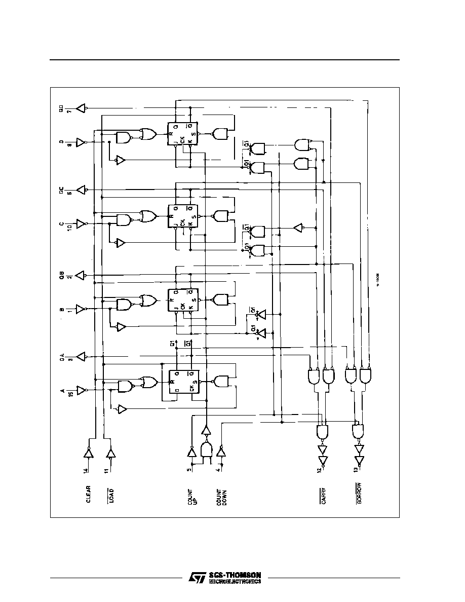
The M54/74HC192/193 are ahigh speed CMOSSYN-
CHRONOUS UP/DOWN DECADE COUNTERS fab-
ricated in silicon gate C
2
MOS technology. They have
the same high speed performance of LSTTL combined
with true CMOS low power consumption. The counter
has two separate clock inputs, an UP COUNT input
and a DOWN COUNT input. All outputs of the flip-flop
are simultaneously triggered on the low to high transi-
tion of either clock while the other input isheld high. The
direction of counting is determined by which input is
clocked. This counter may be preset by entering the
desired data on the DATA A, DATA B, DATA C, and
DATA D input. When the LOAD input is taken low the
data is loaded independently of either clock input. This
feature allows the counters to be used as divide-by-n
counters by modifying the count length with the preset
inputs. In addition the counter can also be cleared. This
is accomplished by inputting a high on the CLEAR
input. All 4 internal stages are set to low independently
of either COUNT input. Both a BORROW and CARRY
output are provided to enable cascading of both up and
down counting functions. The BORROW output pro-
duces a negative going pulse when the counter under-
flows and the CARRY outputs a pulse when the
counter overflows. The counter can be cascaded by
connecting the CARRY and BORROW outputs of one
device to the COUNT UP and COUNT DOWN inputs,
respectively, of the next device. All inputs are equipped
with protection circuits against static discharge and
transient excess voltage.
1/15
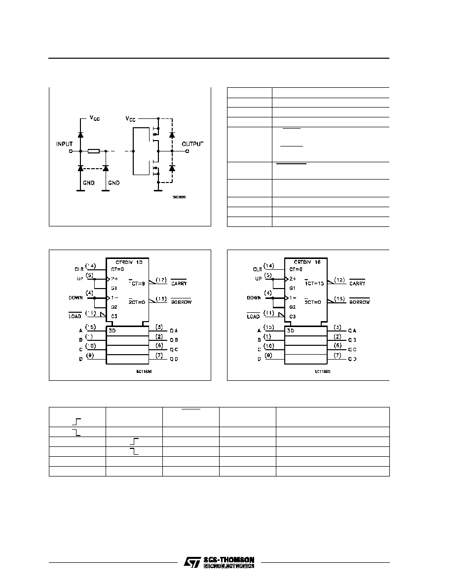
INPUT AND OUTPUT EQUIVALENT CIRCUIT
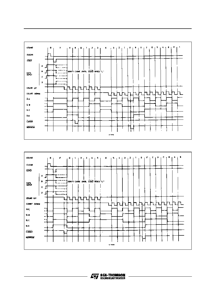
TRUTH TABLE
COUNT UP
COUNT DOWN
LOAD
CLEAR
FUNCTION
H
H
L
COUNT UP
H
H
L
NO COUNT
H
H
L
COUNT DOWN
H
H
L
NO COUNT
X
X
L
L
PRESET
X
X
X
H
RESET
X: Don't Care
PIN DESCRIPTION
PIN No
SYMBOL
NAME AND FUNCTION
3, 2, 6, 7
QA to QD
Flip-Flop Outputs
4
CP
D
Count Down Clock Input
5
CP
U
Count Up Clock Input
11
LOAD
Asynchronous Parallel
Load Input (Active LOW)
12
CARRY
Count Up (Carry)
Output (Active LOW)
13
BORROW
Count Down (Borrow)
Output (Active LOW)
14
CLEAR
Asynchronous Reset
Input (Active HIGH)
15, 1, 10, 9
DA to DD
Data Inputs
8
GND
Ground (0V)
16
V
CC
Positive Supply Voltage
IEC LOGIC SYMBOL (HC193)
IEC LOGIC SYMBOL (HC191)
M54/M74HC192/193
2/15