 | –≠–ª–µ–∫—Ç—Ä–æ–Ω–Ω—ã–π –∫–æ–º–ø–æ–Ω–µ–Ω—Ç: 74AC174M | –°–∫–∞—á–∞—Ç—å:  PDF PDF  ZIP ZIP |
74AC174
HEX D-TYPE FLIP FLOP WITH CLEAR
PRELIMINARY DATA
May 1997
s
HIGH SPEED:
f
MAX
=125 MHz (TYP.) at V
CC
= 5V
s
LOW POWER DISSIPATION:
I
CC
= 8
µ
A (MAX.) at T
A
= 25
o
C
s
HIGH NOISE IMMUNITY:
V
NIH
= V
NIL
= 28% V
CC
(MIN.)
s
50
TRANSMISSION LINE DRIVING
CAPABILITY
s
SYMMETRICAL OUTPUT IMPEDANCE:
|I
OH
| = I
OL
= 24 mA (MIN)
s
BALANCED PROPAGATION DELAYS:
t
PLH
t
PHL
s
OPERATING VOLTAGE RANGE:
V
CC
(OPR) = 2V to 6V
s
PIN AND FUNCTION COMPATIBLE WITH
74 SERIES 174
s
IMPROVED LATCH-UP IMMUNITY
DESCRIPTION
The AC174 is an high-speed CMOS HEX
D-TYPE FLIP FLOP WITH CLEAR fabricated
with sub-micron silicon gate and double-layer
metal wiring C
2
MOS technology. It is ideal for low
power
applications
mantaining
high
speed
operation similar to eqivalent Bipolar Schottky
TTL.
Information signals applied to D inputs are
transfered to the Q output on the positive going
edge of the clock pulse.
When the CLEAR input is held low, the Q outputs
are held low independentelyof the other inputs .
All
inputs and
outputs
are
equipped with
protection circuits against static discharge, giving
them 2KV ESD immunity and transient excess
voltage.
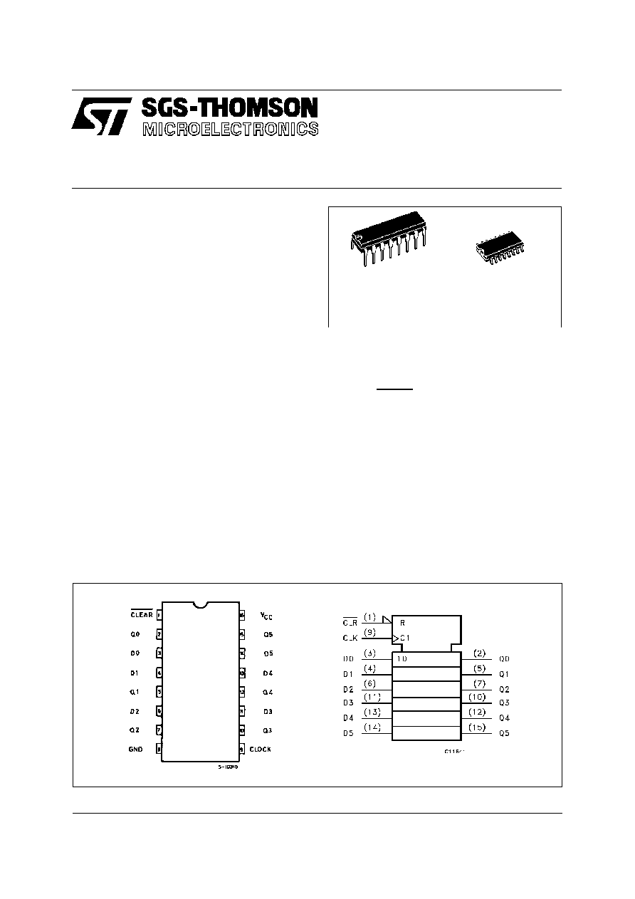
PIN CONNECTION AND IEC LOGIC SYMBOLS
M
(Micro Package)
B
(Plastic Package)
ORDER CODES :
74AC174B
74AC174M
1/10
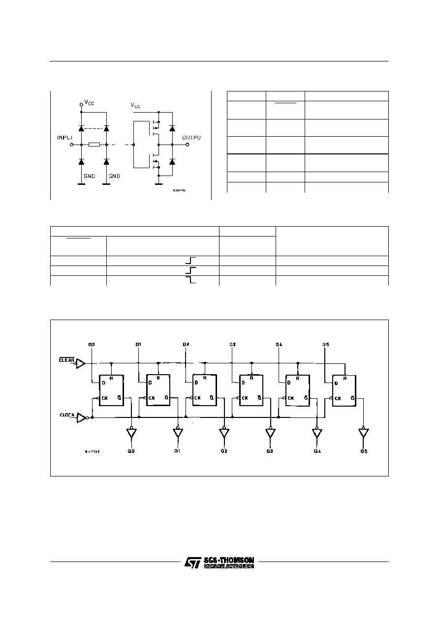
INPUT AND OUTPUT EQUIVALENT CIRCUIT
LOGIC DIAGRAM
PIN DESCRIPTION
PIN No
SYMBOL
NAME AND F UNCTIO N
1
CLEAR
Asyncronous Master Reset
(Active LOW)
2, 5, 7, 10,
12, 15
Q0 to Q5
Flip-Flop Outpus
3, 4, 6, 11,
13, 14
D0 to D5
Data Inputs
9
CLOCK
Clock Input (LOW-to-HIGH,
Edge- Triggered)
8
GND
Ground (0V)
16
V
CC
Positive Supply Voltage
TRUTH TABLE
INPUTS
O UTPUTS
FUNCTI ON
CL EAR
D
CLOCK
Q
L
X
X
L
CLEAR
H
L
L
H
H
H
H
X
Q
n
NO CHANGE
X: Don't Care
This logic diagram has not be used to estimate propagation delays
74AC174
2/10
ABSOLUTE MAXIMUM RATINGS
Symbol
Parameter
Val ue
Uni t
V
CC
Supply Voltage
-0.5 to +7
V
V
I
DC Input Voltage
-0.5 to V
CC
+ 0.5
V
V
O
DC Output Voltage
-0.5 to V
CC
+ 0.5
V
I
IK
DC Input Diode Current
±
20
mA
I
OK
DC Output Diode Current
±
20
mA
I
O
DC Output Current
±
50
mA
I
CC
or I
GND
DC V
CC
or Ground Current
±
300
mA
T
stg
Storage Temperature
-65 to +150
o
C
T
L
Lead Temperature (10 sec)
300
o
C
Absolute Maximum Ratings are those values beyond which damage to the device may occur. Functional operation under these condition is not implied.
RECOMMENDED OPERATING CONDITIONS
Symbol
Parameter
Value
Un it
V
CC
Supply Voltage
2 to 6
V
V
I
Input Voltage
0 to V
CC
V
V
O
Output Voltage
0 to V
CC
V
T
op
Operating Temperature:
-40 to +85
o
C
dt/dv
Input Rise and Fall Time V
CC
= 3.0, 4.5 or 5.5 V(note 1)
8
ns/V
1) V
IN
from 30% to 70% of V
CC
74AC174
3/10
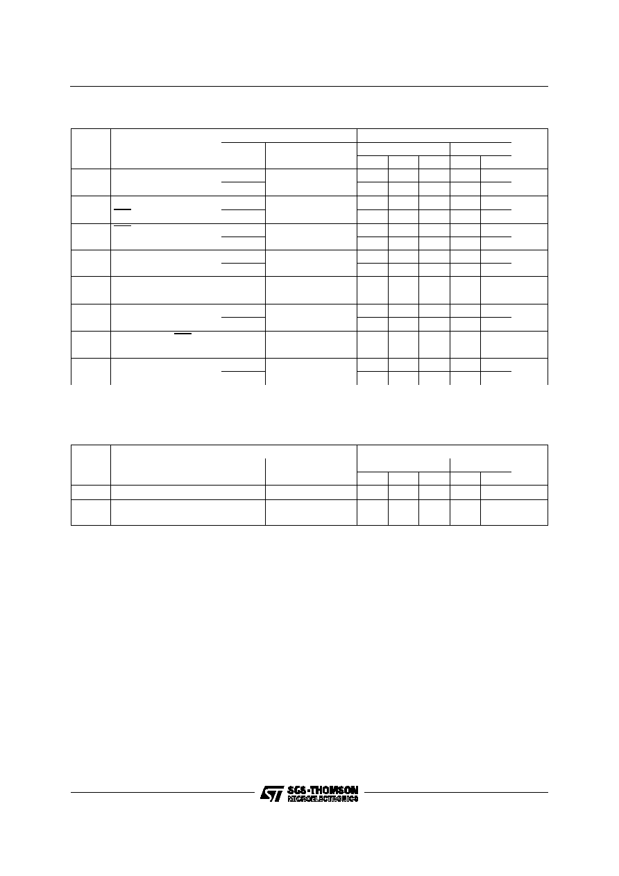
DC SPECIFICATIONS
Symbol
Parameter
Test Con dition s
Value
Unit
V
CC
(V)
T
A
= 25
o
C
-40 to 85
o
C
Mi n.
Typ.
Max.
Min .
Max.
V
IH
High Level Input Voltage
3.0
V
O
= 0.1 V or
V
CC
- 0.1 V
2.1
1.5
2.1
V
4.5
3.15
2.25
3.15
5.5
3.85
2.75
3.85
V
IL
Low Level Input Voltage
3.0
V
O
= 0.1 V or
V
CC
- 0.1 V
1.5
0.9
0.9
V
4.5
2.25
1.35
1.35
5.5
2.75
1.65
1.65
V
OH
High Level Output Voltage
3.0
V
I
(*)
=
V
IH
or
V
IL
I
O
=-50
µ
A
2.9
2.99
2.9
V
4.5
I
O
=-50
µ
A
4.4
4.49
4.4
5.5
I
O
=-50
µ
A
5.4
5.49
5.4
3.0
I
O
=-12 mA
2.56
2.46
4.5
I
O
=-24 mA
3.86
3.76
5.5
I
O
=-24 mA
4.86
4.76
V
OL
Low Level Output Voltage
3.0
V
I
(*)
=
V
IH
or
V
IL
I
O
=50
µ
A
0.002
0.1
0.1
V
4.5
I
O
=50
µ
A
0.001
0.1
0.1
5.5
I
O
=50
µ
A
0.001
0.1
0.1
3.0
I
O
=12 mA
0.36
0.44
4.5
I
O
=24 mA
0.36
0.44
5.5
I
O
=24 mA
0.36
0.44
I
I
Input Leakage Current
5.5
V
I
= V
CC
or GND
±
0.1
±
1
µ
A
I
CC
Quiescent Supply Current
5.5
V
I
= V
CC
or GND
8
80
µ
A
I
OLD
Dynamic Output Current
(note 1, 2)
5.5
V
OLD
= 1.65 V max
75
mA
I
OHD
V
OHD
= 3.85 V min
-75
mA
1) Maximum test duration 2ms, one output loaded at time
2) Incident wave switching is guaranteed on transmission lines with impedances as low as 50
.
(*) All outputs loaded.
74AC174
4/10
AC ELECTRICAL CHARACTERISTICS (C
L
= 50 pF, R
L
= 500
, Input t
r
= t
f
=3 ns)
Symbol
Parameter
T est Cond iti on
Value
Unit
V
CC
(V)
T
A
= 25
o
C
-40 to 85
o
C
Mi n.
Typ.
Max.
Min .
Max.
t
PLH
t
PHL
Propagation Delay Time
CK to Q
3.3
(*)
1.5
8.5
11.0
12.0
ns
5.0
(**)
1.5
6.0
8.0
9.0
t
PLH
t
PHL
Propagation Delay Time
CLR to Q
3.3
(*)
1.5
9.0
11.0
12.0
ns
5.0
(**)
1.5
7.0
9.0
10.0
t
wL
CLR pulse Width, LOW
3.3
(*)
1.0
5.5
7.0
ns
5.0
(**)
1.0
5.0
5.0
t
w
CK pulse Width
3.3
(*)
1.0
5.5
7.0
ns
5.0
(**)
1.0
5.0
5.0
t
s
Setup Time Q to CK HIGH
or LOW
3.3
(*)
2.5
6.5
7.0
ns
5.0
(**)
2.0
5.0
5.5
t
h
Hold Time Q to CK HIGH
or LOW
3.3
(*)
1.0
3.0
3.0
ns
5.0
(**)
0.5
3.0
3.0
t
REM
Recovery Time CLR to CK
3.3
(*)
0
2.5
2.5
ns
5.0
(**)
0
2.0
2.0
f
MAX
Maximum Clock Frequency
3.3
(*)
90
100
70
MHz
5.0
(**)
100
125
100
(*) Voltage range is 3.3V
±
0.3V
(**) Voltage range is 5V
±
0.5V
CAPACITIVE CHARACTERISTICS
Symbol
Parameter
Test Con dition s
Value
Unit
V
CC
(V)
T
A
= 25
o
C
-40 to 85
o
C
Mi n.
Typ.
Max.
Min .
Max.
C
IN
Input Capacitance
5.0
4
pF
C
PD
Power Dissipation
Capacitance (note 1)
5.0
f
IN
= 10 MHz
TBD
pF
1) C
PD
is defined as the value of the IC's internal equivalent capacitance which is calculated from the operating current consumption without load. (Refer to
Test Circuit). Average operting current can be obtained by the following equation. I
CC
(opr) = C
PD
∑
V
CC
∑
f
IN
+ I
CC
/n (per circuit)
74AC174
5/10