 | –≠–ª–µ–∫—Ç—Ä–æ–Ω–Ω—ã–π –∫–æ–º–ø–æ–Ω–µ–Ω—Ç: 74AC244 | –°–∫–∞—á–∞—Ç—å:  PDF PDF  ZIP ZIP |
74AC244
OCTAL BUS BUFFER
WITH 3 STATE OUTPUTS (NON INVERTED)
April 1997
s
HIGH SPEED: t
PD
= 4 ns (TYP.) at V
CC
= 5V
s
LOW POWER DISSIPATION:
I
CC
= 8
µ
A (MAX.) at T
A
= 25
o
C
s
HIGH NOISE IMMUNITY:
V
NIH
= V
NIL
= 28% V
CC
(MIN.)
s
50
TRANSMISSION LINE DRIVING
CAPABILITY
s
SYMMETRICAL OUTPUT IMPEDANCE:
|I
OH
| = I
OL
= 24 mA (MIN)
s
BALANCED PROPAGATION DELAYS:
t
PLH
t
PHL
s
OPERATING VOLTAGE RANGE:
V
CC
(OPR) = 2V to 6V
s
PIN AND FUNCTION COMPATIBLE WITH
74 SERIES 244
s
IMPROVED LATCH-UP IMMUNITY
DESCRIPTION
The AC244 is an advanced CMOS OCTAL BUS
BUFFER (3-STATE) fabricated with sub-micron
silicon gate and double-layer metal wiring C
2
MOS
technology. It is ideal for low power applications
mantaining high speed operation similar to
equivalent Bipolar Schottky TTL.
G control output governs four BUS BUFFERs.
This device is desibned to be used with 3 state
memory address drivers, etc.
All
inputs and
outputs
are
equipped with
protection circuits against static discharge, giving
them 2KV ESD immunity and transient excess
voltage.
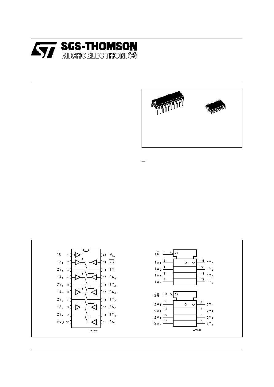
PIN CONNECTION AND IEC LOGIC SYMBOLS
M
(Micro Package)
B
(Plastic Package)
ORDER CODES :
74AC244B
74AC244M
1/8
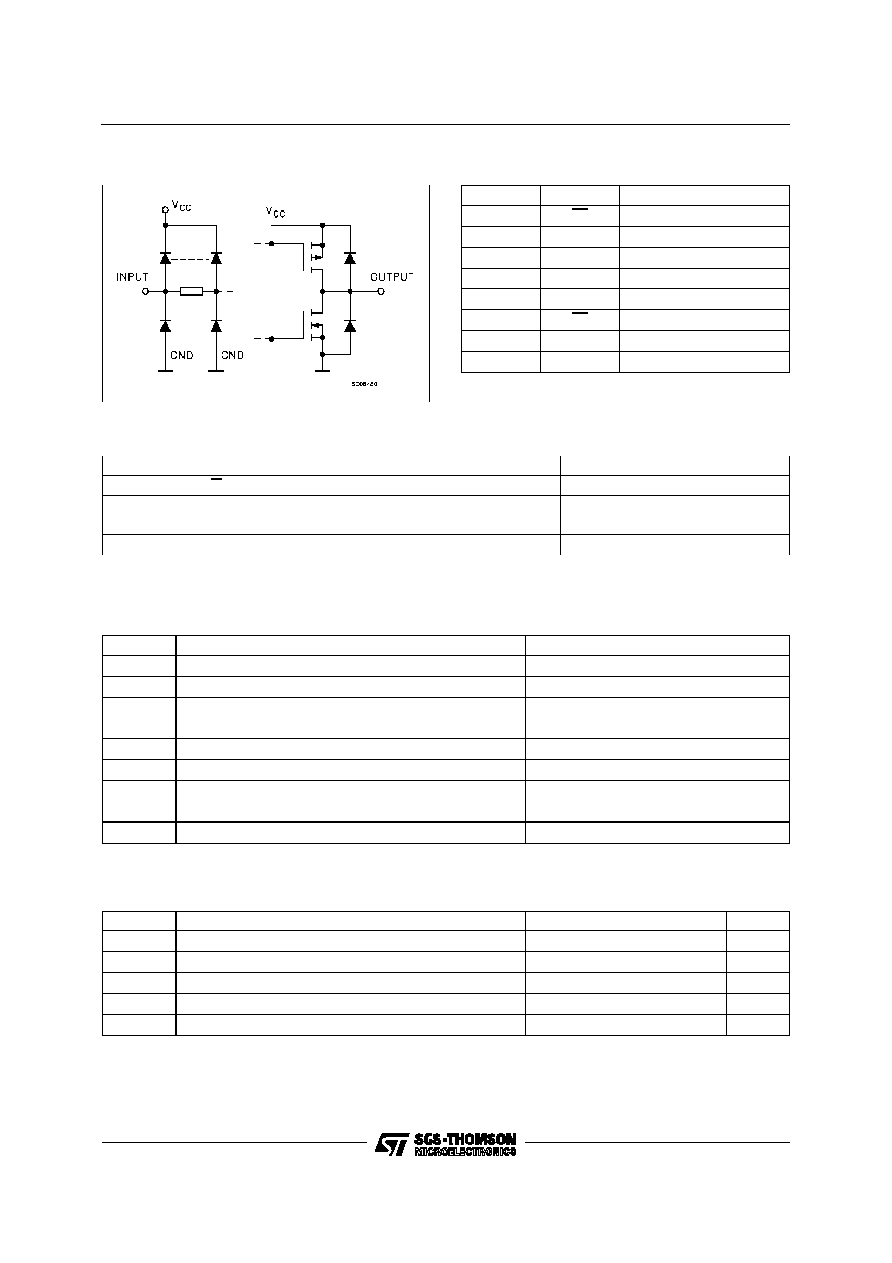
INPUT AND OUTPUT EQUIVALENT CIRCUIT
TRUTH TABLE
INPUT
OUT PUT
G
An
Yn
L
L
L
L
H
H
H
X
Z
X: "H" or "L"
Z: High impedance
PIN DESCRIPTION
PIN No
SYMBOL
NAME AND F UNCTIO N
1
1G
Output Enable Input
2, 4, 6, 8
1A1 to 1A4
Data Inputs
9, 7, 5, 3
2Y1 to 2Y4
Data Outputs
11, 13, 15, 17
2A1 to 2A4
Data Inputs
18, 16, 14, 12
1Y1 to 1Y4
Data Outputs
19
2G
Output Enabel Input
10
GND
Ground (0V)
20
V
CC
Positive Supply Voltage
ABSOLUTE MAXIMUM RATINGS
Symbol
Parameter
Val ue
Uni t
V
CC
Supply Voltage
-0.5 to +7
V
V
I
DC Input Voltage
-0.5 to V
CC
+ 0.5
V
V
O
DC Output Voltage
-0.5 to V
CC
+ 0.5
V
I
IK
DC Input Diode Current
±
20
mA
I
OK
DC Output Diode Current
±
20
mA
I
O
DC Output Current
±
50
mA
I
CC
or I
GND
DC V
CC
or Ground Current
±
400
mA
T
stg
Storage Temperature
-65 to +150
o
C
T
L
Lead Temperature (10 sec)
300
o
C
Absolute Maximum Ratings are those values beyond which damage to the device may occur. Functional operation under these condition is not implied.
RECOMMENDED OPERATING CONDITIONS
Symbol
Parameter
Value
Un it
V
CC
Supply Voltage
2 to 6
V
V
I
Input Voltage
0 to V
CC
V
V
O
Output Voltage
0 to V
CC
V
T
op
Operating Temperature:
-40 to +85
o
C
dt/dv
Input Rise and Fall Time V
CC
= 3.0, 4.5 or 5.5 V(note 1)
8
ns/V
1) V
IN
from 30% to 70% of V
CC
74AC244
2/8
DC SPECIFICATIONS
Symbol
Parameter
Test Con dition s
Value
Unit
V
CC
(V)
T
A
= 25
o
C
-40 to 85
o
C
Mi n.
Typ.
Max.
Min .
Max.
V
IH
High Level Input Voltage
3.0
V
O
= 0.1 V or
V
CC
- 0.1 V
2.1
1.5
2.1
V
4.5
3.15
2.25
3.15
5.5
3.85
2.75
3.85
V
IL
Low Level Input Voltage
3.0
V
O
= 0.1 V or
V
CC
- 0.1 V
1.5
0.9
0.9
V
4.5
2.25
1.35
1.35
5.5
2.75
1.65
1.65
V
OH
High Level Output
Voltage
3.0
V
I
(*)
=
V
IH
or
V
IL
I
O
=-50
µ
A
2.9
2.99
2.9
V
4.5
I
O
=-50
µ
A
4.4
4.49
4.4
5.5
I
O
=-50
µ
A
5.4
5.49
5.4
3.0
I
O
=-12 mA
2.56
2.46
4.5
I
O
=-24 mA
3.86
3.76
5.5
I
O
=-24 mA
4.86
4.76
V
OL
Low Level Output
Voltage
3.0
V
I
(*)
=
V
IH
or
V
IL
I
O
=50
µ
A
0.002
0.1
0.1
V
4.5
I
O
=50
µ
A
0.001
0.1
0.1
5.5
I
O
=50
µ
0.001
0.1
0.1
3.0
I
O
=12 mA
0.36
0.44
4.5
I
O
=24 mA
0.36
0.44
5.5
I
O
=24 mA
0.36
0.44
I
I
Input Leakage Current
5.5
V
I
= V
CC
or GND
±
0.1
±
1
µ
A
I
OZ
3 State Output Leakage
Current
5.5
V
I
= V
IH
or V
IL
V
O
= V
CC
or GND
±
0.5
±
5
µ
A
I
CC
Quiescent Supply
Current
5.5
V
I
= V
CC
or GND
8
80
µ
A
I
OLD
Dynamic Output Current
(note 1, 2)
5.5
V
OLD
= 1.65 V max
75
mA
I
OHD
V
OHD
= 3.85 V min
-75
mA
1) Maximum test duration 2ms, one output loaded at time
2) Incident wave switching is guaranteed on transmission lines with impedances as low as 50
.
(*) All outputs loaded.
74AC244
3/8
CAPACITIVE CHARACTERISTICS
Symb ol
Parameter
Test Cond iti on s
Value
Un it
V
CC
(V)
T
A
= 25
o
C
-40 to 85
o
C
Min .
Typ.
Max.
Min.
Max.
C
IN
Input Capacitance
5.0
4
pF
C
OUT
Output Capacitance
5.0
8
pF
C
PD
Power Dissipation
Capacitance (note 1)
5.0
21
pF
1) C
PD
is defined as the value of the IC's internal equivalent capacitance which is calculated from the operating current consumption without load. (Refer to
Test Circuit). Average operating current can be obtained by the following equation. I
CC
(opr) = C
PD
∑
V
CC
∑
f
IN
+ I
CC
/n (per circuit)
AC ELECTRICAL CHARACTERISTICS (C
L
= 50 pF, R
L
= 500
, Input t
r
= t
f
=3 ns)
Symbol
Parameter
T est Cond iti on
Value
Unit
V
CC
(V)
T
A
= 25
o
C
-40 to 85
o
C
Mi n.
Typ.
Max.
Min .
Max.
t
PLH
t
PHL
Propagation Delay Time
3.3
(*)
1.5
5
9
1.5
10
ns
5.0
(**)
1.5
4
7
1.5
7.5
t
PZL
t
PZH
Output Enable Time
3.3
(*)
1.5
6
10
1.5
11
ns
5.0
(**)
1.5
4
8
1.5
8.5
t
PLZ
t
PHZ
Output Disable Time
3.3
(*)
1.5
7
11
1.5
12
ns
5.0
(**)
1.5
5.5
9
1.5
10
(*) Voltage range is 3.3V
±
0.3V
(**) Voltage range is 5V
±
0.5V
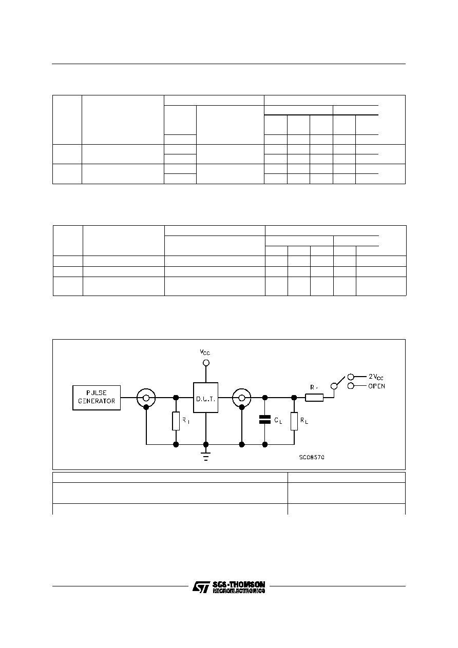
TEST CIRCUIT
TEST
SWI TCH
t
PLH
, t
PHL
Open
t
PZL
, t
PLZ
2V
CC
t
PZH
, t
PHZ
Open
C
L
= 50 pF or equivalent (includes jig and probe capacitance)
R
L
= R
1
= 500
or equivalent
R
T
= Z
OUT
of pulse generator (typically 50
)
74AC244
4/8
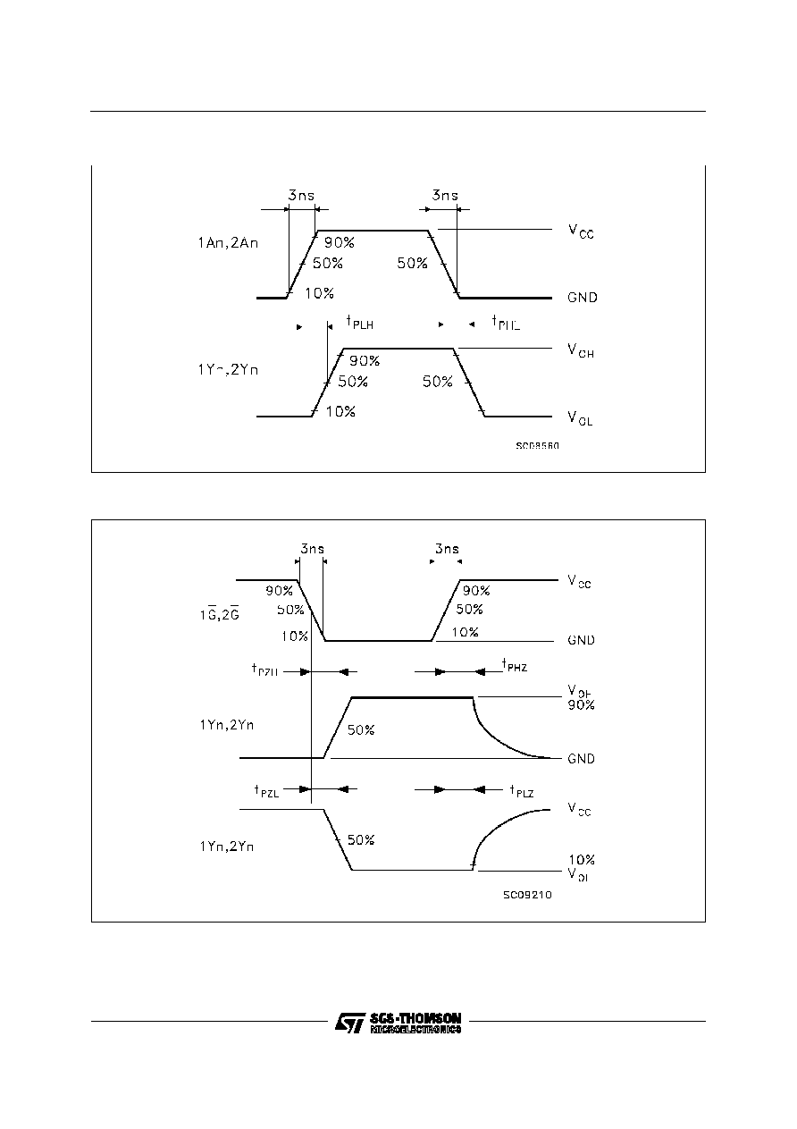
WAVEFORM 1: PROPAGATION DELAYS (f=1MHz; 50% duty cycle)
WAVEFORM 2: OUTPUT ENABLE AND DISABLE TIME (f=1MHz; 50% duty cycle)
74AC244
5/8