 | –≠–ª–µ–∫—Ç—Ä–æ–Ω–Ω—ã–π –∫–æ–º–ø–æ–Ω–µ–Ω—Ç: 74AC273 | –°–∫–∞—á–∞—Ç—å:  PDF PDF  ZIP ZIP |
74AC273
OCTAL D-TYPE FLIP FLOP WITH CLEAR
PRELIMINARY DATA
Æ
November 1998
s
HIGH SPEED:
f
MAX
= 190 MHz (TYP.) at V
CC
= 5V
s
LOW POWER DISSIPATION:
I
CC
= 8
µ
A (MAX.) at T
A
= 25
o
C
s
HIGH NOISE IMMUNITY:
V
NIH
= V
NIL
= 28% V
CC
(MIN.)
s
50
TRANSMISSION LINE DRIVING
CAPABILITY
s
SYMMETRICAL OUTPUT IMPEDANCE:
|I
OH
| = I
OL
= 24 mA (MIN)
s
BALANCED PROPAGATION DELAYS:
t
PLH
t
PHL
s
OPERATING VOLTAGE RANGE:
V
CC
(OPR) = 2V to 6V
s
PIN AND FUNCTION COMPATIBLE WITH
74 SERIES 273
s
IMPROVED LATCH-UP IMMUNITY
DESCRIPTION
The AC273 is a high-speed CMOS OCTAL
D-TYPE FLIP FLOP WITH
CLEAR fabricated
with sub-micron silicon gate and double-layer
metal wiring C
2
MOS technology. It is ideal for low
power
applications
mantaining
high
speed
operation similar to equivalent Bipolar Schottky
TTL.
Information signals applied to D inputs are
transfered to the Q output on the positive going
edge of the clock pulse.
When the CLEAR input is held low, the Q outputs
are held low independentely of the other inputs .
All inputs
and
outputs are
equipped with
protection circuits against static discharge, giving
them 2KV ESD immunity and transient excess
voltage.
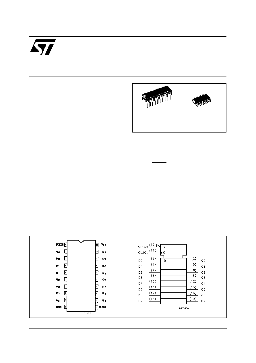
PIN CONNECTION AND IEC LOGIC SYMBOLS
M
(Micro Package)
B
(Plastic Package)
ORDER CODES :
74AC273B
74AC273M
1/10
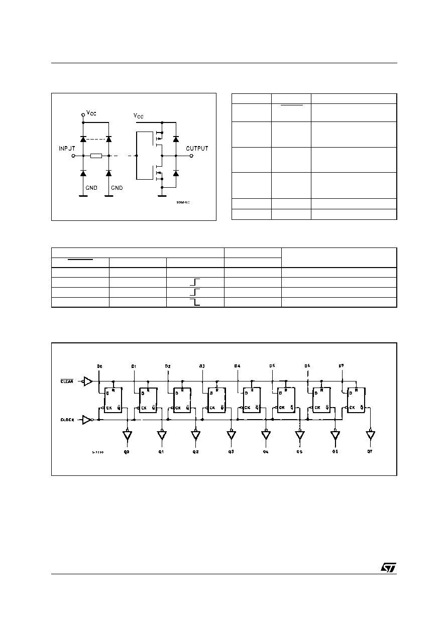
INPUT AND OUTPUT EQUIVALENT CIRCUIT
LOGIC DIAGRAMS
PIN DESCRIPTION
PIN No
SYMBOL
NAME AND FUNCT ION
1
CLEAR
Asyncronous Master
Reset (Active LOW)
2, 5, 6, 9,
12, 15, 16,
19
Q0 to Q7
Flip-Flop Outpus
3, 4, 7, 8,
13, 14, 17,
18
D0 to D7
Data Inputs
11
CLOCK
Clock Input
(LOW-to-HIGH, Edge-
Triggered)
10
GND
Ground (0V)
20
V
CC
Positive Supply Voltage
TRUTH TABLE
I NPUTS
OUT PUT S
F UNCTIO N
CL EAR
D
CLO CK
Q
L
X
X
L
CLEAR
H
L
L
H
H
H
H
X
Q
n
NO CHANGE
X:Don't Care
Thislogic diagram has notbe used to esimate propagation delays
74AC273
2/10

ABSOLUTE MAXIMUM RATINGS
Symbol
Parameter
Val ue
Unit
V
CC
Supply Voltage
-0.5 to +7
V
V
I
DC Input Voltage
-0.5 to V
CC
+ 0.5
V
V
O
DC Output Voltage
-0.5 to V
CC
+ 0.5
V
I
IK
DC Input Diode Current
±
20
mA
I
OK
DC Output Diode Current
±
20
mA
I
O
DC Output Current
±
50
mA
I
CC
or I
GND
DC V
CC
or Ground Current
±
400
mA
T
stg
Storage Temperature
-65 to +150
o
C
T
L
Lead Temperature (10 sec)
300
o
C
Absolute Maximum Ratings are those values beyond which damage to the device may occur. Functional operation under these condition is not implied.
RECOMMENDED OPERATING CONDITIONS
Symbol
Parameter
Valu e
Uni t
V
CC
Supply Voltage
2 to 6
V
V
I
Input Voltage
0 to V
CC
V
V
O
Output Voltage
0 to V
CC
V
T
op
Operating Temperature:
-40 to +85
o
C
dt/dv
Input Rise and Fall Time V
CC
= 3.0, 4.5 or 5.5 V(note 1)
8
ns/V
1) V
IN
from 30% to70%of V
CC
74AC273
3/10

DC SPECIFICATIONS
Symb ol
Parameter
Test Co nditi ons
Valu e
Un it
V
CC
(V)
T
A
= 25
o
C
-40 to 85
o
C
Min.
T yp.
Max.
Mi n.
Max.
V
IH
High Level Input Voltage
3.0
V
O
= 0.1 V or
V
CC
- 0.1 V
2.1
1.5
2.1
V
4.5
3.15
2.25
3.15
5.5
3.85
2.75
3.85
V
IL
Low Level Input Voltage
3.0
V
O
= 0.1 V or
V
CC
- 0.1 V
1.5
0.9
0.9
V
4.5
2.25
1.35
1.35
5.5
2.75
1.65
1.65
V
OH
High Level Output
Voltage
3.0
V
I
(* )
=
V
IH
or
V
IL
I
O
=-50
µ
A
2.9
2.99
2.9
V
4.5
I
O
=-50
µ
A
4.4
4.49
4.4
5.5
I
O
=-50
µ
A
5.4
5.49
5.4
3.0
I
O
=-12 mA
2.56
2.46
4.5
I
O
=-24 mA
3.86
3.76
5.5
I
O
=-24 mA
4.86
4.76
V
OL
Low Level Output
Voltage
3.0
V
I
(* )
=
V
IH
or
V
IL
I
O
=50
µ
A
0.002
0.1
0.1
V
4.5
I
O
=50
µ
A
0.001
0.1
0.1
5.5
I
O
=50
µ
A
0.001
0.1
0.1
3.0
I
O
=12 mA
0.36
0.44
4.5
I
O
=24 mA
0.36
0.44
5.5
I
O
=24 mA
0.36
0.44
I
I
Input Leakage Current
5.5
V
I
= V
CC
or GND
±
0.1
±
1
µ
A
I
CC
Quiescent Supply
Current
5.5
V
I
= V
CC
or GND
8
80
µ
A
I
OLD
Dynamic Output Current
(note 1, 2)
5.5
V
OLD
= 1.65 V max
75
mA
I
OHD
V
OHD
= 3.85 V min
-75
mA
1) Maximum test duration 2ms, one output loaded attime
2) Incident wave switching is guaranteed on transmission lines with impedances as low as 50
.
(*) All outputs loaded.
74AC273
4/10

AC ELECTRICAL CHARACTERISTICS (C
L
= 50 pF, R
L
= 500
, Input t
r
= t
f
=3 ns)
Symb ol
Parameter
T est Con ditio n
Valu e
Un it
V
CC
(V)
T
A
= 25
o
C
-40 to 85
o
C
Min.
T yp.
Max.
Mi n.
Max.
t
PLH
t
PHL
Propagation Delay Time
CLOCK to Q
3.3
(*)
4.0
8.0
12.5
3.0
14.0
ns
5.0
(*)
3.0
5.5
9.0
2.5
10.0
t
PHL
Propagation Delay Time
CLEAR to Q
3.3
(*)
4.0
8.5
13.0
3.0
14.0
ns
5.0
(**)
3.0
6.5
10.0
2.5
11.0
t
w
CLEAR pulse Width
3.3
(*)
5.5
6.0
ns
5.0
(**)
4.0
4.5
t
w
CLOCK pulse Width
3.3
(*)
5.5
6.0
ns
5.0
(**)
4.0
4.5
t
s
Setup Time D to CK
HIGH or LOW
3.3
(*)
5.5
6.0
ns
5.0
(**)
4.0
4.5
t
h
Hold Time D to CK
HIGH or LOW
3.3
(*)
1.5
1.5
ns
5.0
(**)
1.5
1.5
t
REM
Recovery Time CLEAR
to CLOCK
3.3
(*)
4.0
4.5
ns
5.0
(**)
3.0
3.0
f
MAX
Maximum Clock
Frequency
3.3
(*)
90
75
MHz
5.0
(**)
140
190
125
*) Voltage range is 3.3V
±
0.3V
(**) Voltage range is 5V
±
0.5V
CAPACITIVE CHARACTERISTICS
Symb ol
Parameter
Test Co nditi ons
Valu e
Un it
V
CC
(V)
T
A
= 25
o
C
-40 to 85
o
C
Min.
T yp.
Max.
Mi n.
Max.
C
IN
Input Capacitance
5.0
4
pF
C
PD
Power Dissipation
Capacitance (note 1)
5.0
f
IN
= 10 MHz
TBD
pF
1) C
PD
isdefined as the value of the IC'sinternal equivalent capacitance which is calculated fromthe operating current consumption without load. (Referto
Test Circuit).Average operting current can be obtained by the following equation. I
CC
(opr) = C
PD
∑
V
CC
∑
f
IN
+ I
CC
/n(per circuit)
74AC273
5/10