 | –≠–ª–µ–∫—Ç—Ä–æ–Ω–Ω—ã–π –∫–æ–º–ø–æ–Ω–µ–Ω—Ç: 74AC280M | –°–∫–∞—á–∞—Ç—å:  PDF PDF  ZIP ZIP |
74AC280
9 BIT PARITY GENERATOR
Æ
December 1998
s
HIGH SPEED: t
PD
= 4 ns (TYP.) at V
CC
= 5V
s
LOW POWER DISSIPATION:
I
CC
= 4
µ
A (MAX.) at T
A
= 25
o
C
s
HIGH NOISE IMMUNITY:
V
NIH
= V
NIL
= 28% V
CC
(MIN.)
s
50
TRANSMISSION LINE DRIVING
CAPABILITY
s
SYMMETRICAL OUTPUT IMPEDANCE:
|I
OH
| = I
OL
= 24 mA (MIN)
s
BALANCED PROPAGATION DELAYS:
t
PLH
t
PHL
s
OPERATING VOLTAGE RANGE:
V
CC
(OPR) = 2V to 6V
s
PIN AND FUNCTION COMPATIBLE WITH
74 SERIES 280
s
IMPROVED LATCH-UP IMMUNITY
DESCRIPTION
The AC280 is an advanced high-speed CMOS 9
BIT
PARITY
GENERATOR
fabricated
with
sub-micron silicon gate and double-layer metal
wiring C
2
MOS technology. It is ideal for low
power
applications
mantaining
high
speed
operation similar to equivalent Bipolar Schottky
TTL.
It is composed of nine data inputs (A to I) and
odd/even parity outputs (
ODD and
EVEN). The
nine data inputs control the output conditions.
When the number of high level input is odd,
ODD output is kept high and
EVEN output low.
Conservely, when the output is even,
EVEN
output is kept high and
ODD low.
The IC generates either odd or even parity
making it flexible application.
The word-length capability is easily expanded by
cascading.
All inputs
and
outputs are
equipped with
protection circuits against static discharge, giving
them 2KV ESD immunity and transient excess
voltage.
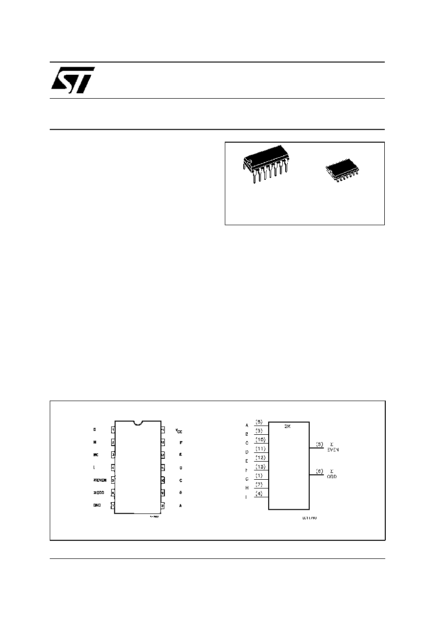
PIN CONNECTION AND IEC LOGIC SYMBOLS
ORDER CODES :
74AC280B
74AC280M
M
(Micro Package)
B
(Plastic Package)
1/8
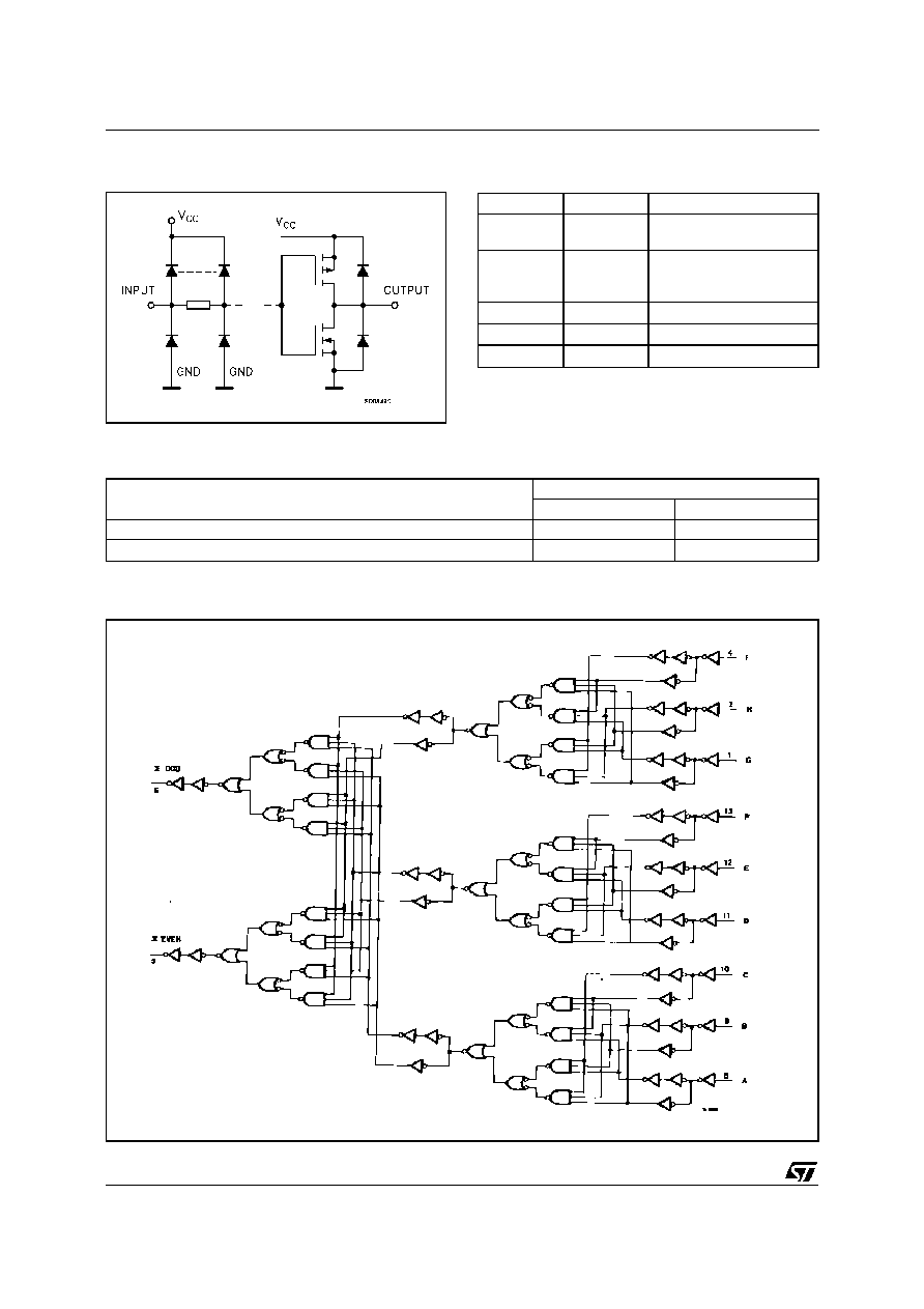
INPUT AND OUTPUT EQUIVALENT CIRCUIT
TRUTH TABLE
NUMBER OF INPUTS A THRU I THAT ARE HIGH
OUTPUT
EVEN
ODD
0, 2, 4, 6, 8
H
L
1, 3, 5, 7, 9
L
H
PIN DESCRIPTION
PI N No
SYMBOL
NAME AND FUNCT ION
5, 6
EVEN
ODD
Parity Outputs
8, 9, 10, 11,
12, 13, 1, 2,
4
A to I
Data Inputs
3
NC
No Connection
7
GND
Ground (0V)
14
V
CC
Positive Supply Voltage
LOGIC DIAGRAM
74AC280
2/8
ABSOLUTE MAXIMUM RATINGS
Symbol
Parameter
Val ue
Unit
V
CC
Supply Voltage
-0.5 to +7
V
V
I
DC Input Voltage
-0.5 to V
CC
+ 0.5
V
V
O
DC Output Voltage
-0.5 to V
CC
+ 0.5
V
I
IK
DC Input Diode Current
±
20
mA
I
OK
DC Output Diode Current
±
20
mA
I
O
DC Output Current
±
50
mA
I
CC
or I
GND
DC V
CC
or Ground Current
±
200
mA
T
stg
Storage Temperature
-65 to +150
o
C
T
L
Lead Temperature (10 sec)
300
o
C
Absolute Maximum Ratings are those values beyond which damage to the device may occur. Functional operation under these condition is not implied.
RECOMMENDED OPERATING CONDITIONS
Symbol
Parameter
Valu e
Uni t
V
CC
Supply Voltage
2 to 6
V
V
I
Input Voltage
0 to V
CC
V
V
O
Output Voltage
0 to V
CC
V
T
op
Operating Temperature:
-40 to +85
o
C
dt/dv
Input Rise and Fall Time V
CC
= 3.0, 4.5 or 5.5 V(note 1)
8
ns/V
1) V
IN
from 30% to70%of V
CC
74AC280
3/8
CAPACITIVE CHARACTERISTICS
Symb ol
Parameter
Test Co nditi ons
Valu e
Un it
V
CC
(V)
T
A
= 25
o
C
-40 to 85
o
C
Min.
T yp.
Max.
Mi n.
Max.
C
IN
Input Capacitance
5.0
4
pF
C
PD
Power Dissipation
Capacitance (note 1)
5.0
27
pF
1) C
PD
isdefined as the value of the IC'sinternal equivalent capacitance which is calculated fromthe operating current consumption without load. (Referto
Test Circuit).Average operating current can be obtained by the following equation. I
CC
(opr) = C
PD
∑
V
CC
∑
f
IN
+ I
CC
AC ELECTRICAL CHARACTERISTICS (C
L
= 50 pF, R
L
= 500
, Input t
r
= t
f
=3 ns)
Symb ol
Parameter
T est Con ditio n
Valu e
Un it
V
CC
(V)
T
A
= 25
o
C
-40 to 85
o
C
Min.
T yp.
Max.
Mi n.
Max.
t
PLH
t
PHL
Propagation Delay Time
(Input -
ODD,
EVEN)
3.3
(*)
1.5
5
17.0
1
18.5
ns
5.0
(**)
1.5
4
13.0
1
14.5
(*) Voltage range is 3.3V
±
0.3V
(**) Voltage range is 5V
±
0.5V
DC SPECIFICATIONS
Symb ol
Parameter
Test Co nditi ons
Valu e
Un it
V
CC
(V)
T
A
= 25
o
C
-40 to 85
o
C
Min.
T yp.
Max.
Mi n.
Max.
V
IH
High Level Input Voltage
3.0
V
O
= 0.1 V or
V
CC
- 0.1 V
2.1
1.5
2.1
V
4.5
3.15
2.25
3.15
5.5
3.85
2.75
3.85
V
IL
Low Level Input Voltage
3.0
V
O
= 0.1 V or
V
CC
- 0.1 V
1.5
0.9
0.9
V
4.5
2.25
1.35
1.35
5.5
2.75
1.65
1.65
V
OH
High Level Output
Voltage
3.0
V
I
(* )
=
V
IH
or
V
IL
I
O
=-50
µ
A
2.9
2.99
2.9
V
4.5
I
O
=-50
µ
A
4.4
4.49
4.4
5.5
I
O
=-50
µ
A
5.4
5.49
5.4
3.0
I
O
=-12 mA
2.56
2.46
4.5
I
O
=-24 mA
3.86
3.76
5.5
I
O
=-24 mA
4.86
4.76
V
OL
Low Level Output
Voltage
3.0
V
I
(* )
=
V
IH
or
V
IL
I
O
=50
µ
A
0.002
0.1
0.1
V
4.5
I
O
=50
µ
A
0.001
0.1
0.1
5.5
I
O
=50
µ
A
0.001
0.1
0.1
3.0
I
O
=12 mA
0.36
0.44
4.5
I
O
=24 mA
0.36
0.44
5.5
I
O
=24 mA
0.36
0.44
I
I
Input Leakage Current
5.5
V
I
= V
CC
or GND
±
0.1
±
1
µ
A
I
CC
Quiescent Supply
Current
5.5
V
I
= V
CC
or GND
4
40
µ
A
I
OLD
Dynamic Output Current
(note 1, 2)
5.5
V
OLD
= 1.65 V max
75
mA
I
OHD
V
OHD
= 3.85 V min
-75
mA
1) Maximum test duration 2ms, one output loaded attime
2) Incident wave switching is guaranteed on transmission lines with impedances as low as 50
.
(*) All outputs loaded.
74AC280
4/8
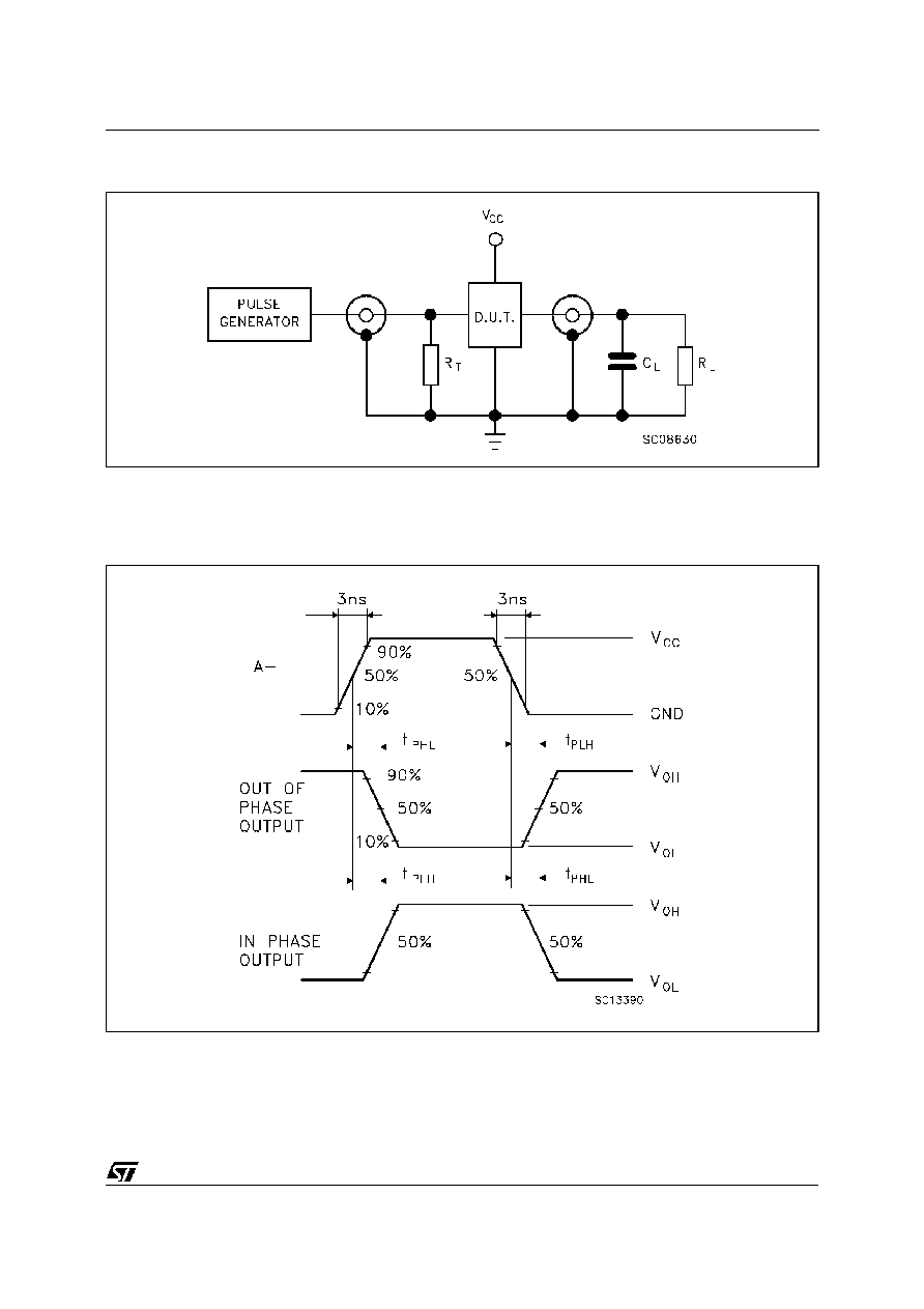
TEST CIRCUIT
C
L
= 50 pF or equivalent (includes jigand probe capacitance)
R
L
= R
1
= 500
orequivalent
R
T
= Z
OUT
of pulse generator (typically 50
)
WAVEFORM: PROPAGATION DELAYS (f=1MHz; 50% duty cycle)
74AC280
5/8