 | –≠–ª–µ–∫—Ç—Ä–æ–Ω–Ω—ã–π –∫–æ–º–ø–æ–Ω–µ–Ω—Ç: 74ACT174 | –°–∫–∞—á–∞—Ç—å:  PDF PDF  ZIP ZIP |
74ACT174
HEX D-TYPE FLIP FLOP WITH CLEAR
PRELIMINARY DATA
May 1997
s
HIGH SPEED:
f
MAX
= 200 MHz (TYP.) at V
CC
= 5V
s
LOW POWER DISSIPATION:
I
CC
= 8
µ
A (MAX.) at T
A
= 25
o
C
s
COMPATIBLE WITH TTL OUTPUTS
V
IH
= 2V (MIN), V
IL
= 0.8V (MAX)
s
50
TRANSMISSION LINE DRIVING
CAPABILITY
s
SYMMETRICAL OUTPUT IMPEDANCE:
|I
OH
| = I
OL
= 24 mA (MIN)
s
BALANCED PROPAGATION DELAYS:
t
PLH
t
PHL
s
OPERATING VOLTAGE RANGE:
V
CC
(OPR) = 4.5V to 5.5V
s
PIN AND FUNCTION COMPATIBLE WITH
74 SERIES 174
s
IMPROVED LATCH-UP IMMUNITY
DESCRIPTION
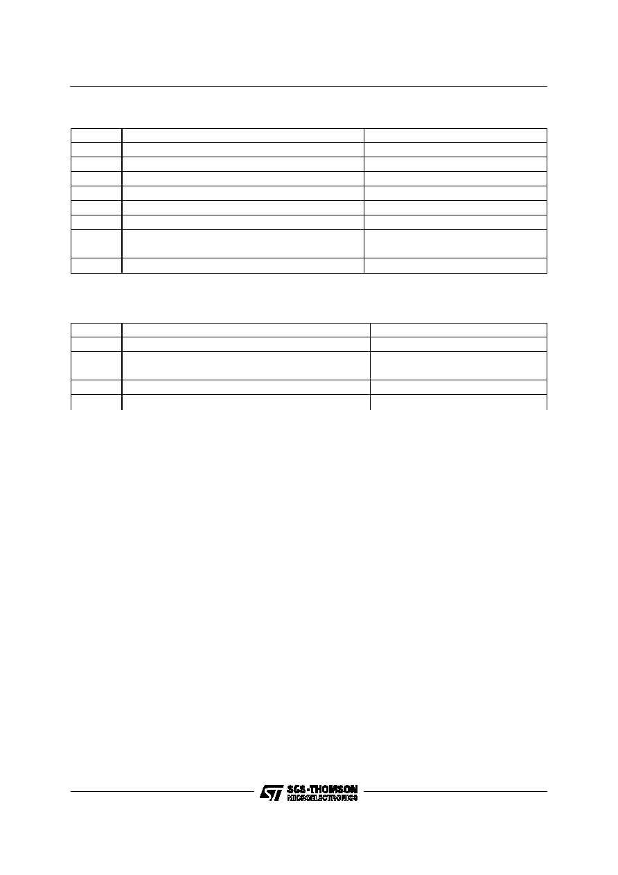
The ACT174 is an high-speed CMOS HEX
D-TYPE FLIP FLOP WITH CLEAR fabricated
with sub-micron silicon gate and double-layer
metal wiring C
2
MOS technology. It is ideal for low
power
applications
mantaining
high
speed
operation similar to eqivalent Bipolar Schottky
TTL.
Information signals applied to D inputs are
transfered to the Q output on the positive going
edge of the clock pulse.
When the CLEAR input is held low, the Q outputs
are held low independentelyof the other inputs .
The device is designed to interface directly High
Speed CMOS systems with TTL, NMOS and
CMOS output voltage levels.
All
inputs and
outputs
are
equipped with
protection circuits against static discharge, giving
them 2KV ESD immunity and transient excess
voltage.
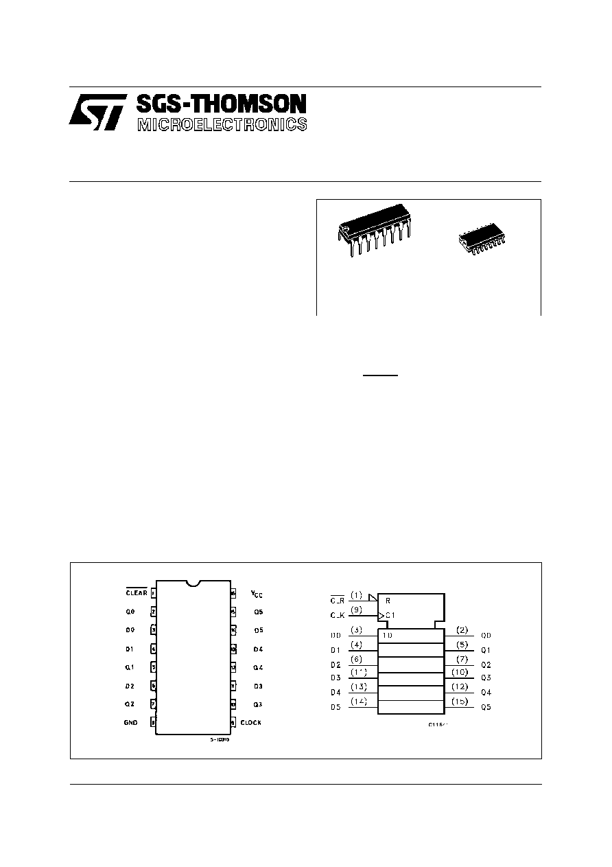
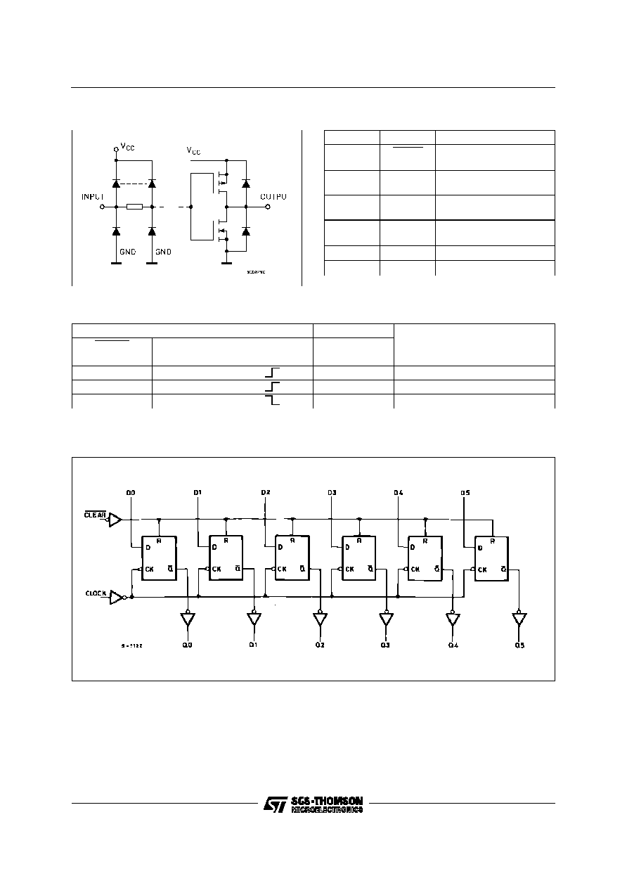
PIN CONNECTION AND IEC LOGIC SYMBOLS
M
(Micro Package)
B
(Plastic Package)
ORDER CODES :
74ACT174B
74ACT174M
1/10
INPUT AND OUTPUT EQUIVALENT CIRCUIT
LOGIC DIAGRAM
PIN DESCRIPTION
PIN No
SYMBOL
NAME AND F UNCTIO N
1
CLEAR
Asyncronous Master Reset
(Active LOW)
2, 5, 7, 10,
12, 15
Q0 to Q5
Flip-Flop Outpus
3, 4, 6, 11,
13, 14
D0 to D5
Data Inputs
9
CLOCK
Clock Input (LOW-to-HIGH,
Edge- Triggered)
8
GND
Ground (0V)
16
V
CC
Positive Supply Voltage
TRUTH TABLE
INPUTS
O UTPUTS
FUNCTI ON
CL EAR
D
CLOCK
Q
L
X
X
L
CLEAR
H
L
L
H
H
H
H
X
Q
n
NO CHANGE
X: Don't Care
This logic diagram has not be used to estimate propagation delays
74ACT174
2/10
ABSOLUTE MAXIMUM RATINGS
Symbol
Parameter
Val ue
Uni t
V
CC
Supply Voltage
-0.5 to +7
V
V
I
DC Input Voltage
-0.5 to V
CC
+ 0.5
V
V
O
DC Output Voltage
-0.5 to V
CC
+ 0.5
V
I
IK
DC Input Diode Current
±
20
mA
I
OK
DC Output Diode Current
±
20
mA
I
O
DC Output Current
±
50
mA
I
CC
or I
GND
DC V
CC
or Ground Current
±
300
mA
T
stg
Storage Temperature
-65 to +150
o
C
T
L
Lead Temperature (10 sec)
300
o
C
Absolute Maximum Ratings are those values beyond which damage to the device may occur. Functional operation under these condition is not implied.
RECOMMENDED OPERATING CONDITIONS
Symbol
Parameter
Valu e
Uni t
V
CC
Supply Voltage
4.5 to 5.5
V
V
I
Input Voltage
0 to V
CC
V
V
O
Output Voltage
0 to V
CC
V
T
op
Operating Temperature:
-40 to +85
o
C
dt/dv
Input Rise and Fall Time V
CC
= 4.5 to 5.5V (note 1)
8
ns/V
1) V
IN
from 0.8 V to 2.0 V
74ACT174
3/10
DC SPECIFICATIONS
Symbol
Parameter
Test Con dition s
Value
Unit
V
CC
(V)
T
A
= 25
o
C
-40 to 85
o
C
Mi n.
Typ.
Max.
Min .
Max.
V
IH
High Level Input Voltage
4.5
V
O
= 0.1 V or
V
CC
- 0.1 V
2.0
1.5
2.0
V
5.5
2.0
1.5
2.0
V
IL
Low Level Input Voltage
4.5
V
O
= 0.1 V or
V
CC
- 0.1 V
1.5
0.8
0.8
V
5.5
1.5
0.8
0.8
V
OH
High Level Output Voltage
4.5
V
I
(*)
=
V
IH
or
V
IL
I
O
=-50
µ
A
4.4
4.49
4.4
V
5.5
I
O
=-50
µ
A
5.4
5.49
5.4
4.5
I
O
=-24 mA
3.86
3.76
5.5
I
O
=-24 mA
4.86
4.76
V
OL
Low Level Output Voltage
4.5
V
I
(*)
=
V
IH
or
V
IL
I
O
=50
µ
A
0.001
0.1
0.1
V
5.5
I
O
=50 mA
0.001
0.1
0.1
4.5
I
O
=24 mA
0.36
0.44
5.5
I
O
=24 mA
0.36
0.44
I
I
Input Leakage Current
5.5
V
I
= V
CC
or GND
±
0.1
±
1
µ
A
I
CCT
Max I
CC
/Input
5.5
V
I
= V
CC
-2.1 V
0.6
1.5
mA
I
CC
Quiescent Supply Current
5.5
V
I
= V
CC
or GND
8
80
µ
A
I
OLD
Dynamic Output Current
(note 1, 2)
5.5
V
OLD
= 1.65 V max
75
mA
I
OHD
V
OHD
= 3.85 V min
-75
mA
1) Maximum test duration 2ms, one output loaded at time
2) Incident wave switching is guaranteed on transmission lines with impedances as low as 50
.
(*) All outputs loaded.
74ACT174
4/10
AC ELECTRICAL CHARACTERISTICS (C
L
= 50 pF, R
L
= 500
, Input t
r
= t
f
=3 ns)
Symbol
Parameter
T est Cond iti on
Value
Unit
V
CC
(V)
T
A
= 25
o
C
-40 to 85
o
C
Mi n.
Typ.
Max.
Min .
Max.
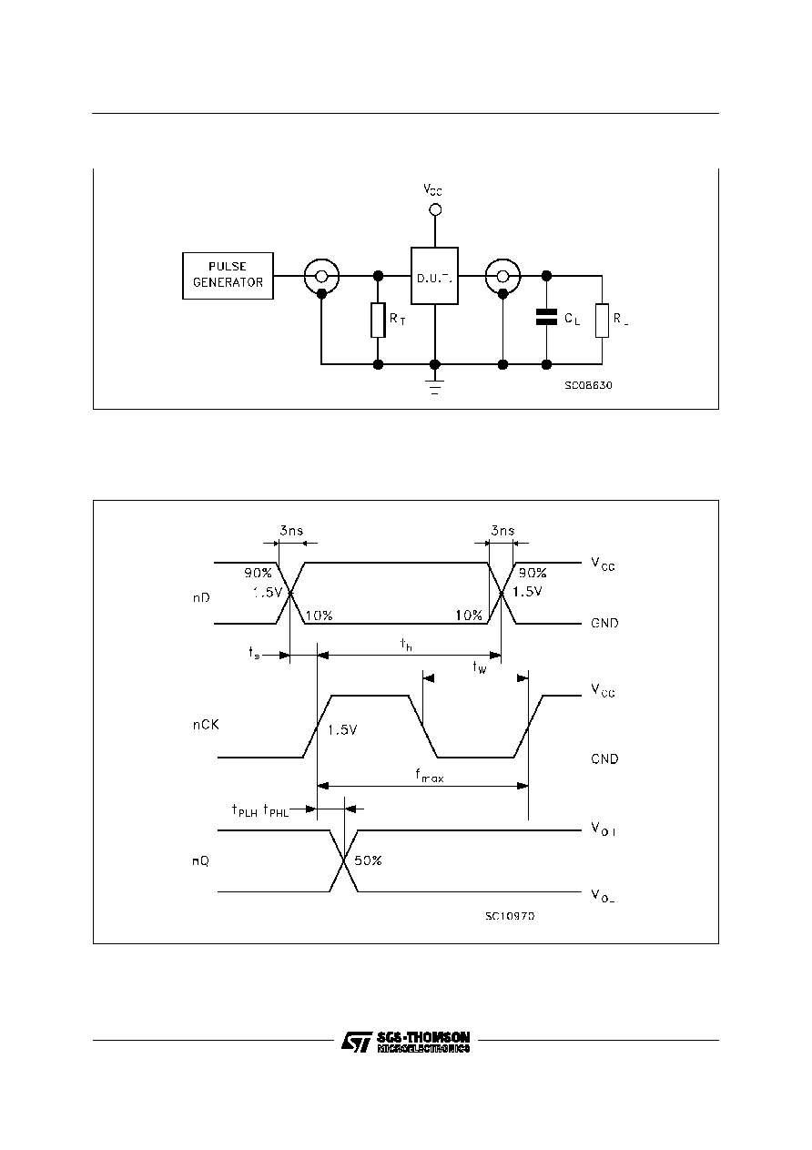
t
PLH
t
PHL
Propagation Delay Time
CK to Q
5.0
(*)
1.5
7.0
10.5
11.5
ns
t
PLH
t
PHL
Propagation Delay Time
CLR to Q
5.0
(*)
1.5
6.5
9.5
11.0
ns
t
wL
CLR pulse Width, LOW
5.0
(*)
1.5
3.0
3.5
ns
t
w
CK pulse Width
5.0
(*)
1.5
3.0
3.5
ns
t
s
Setup Time Q to CK HIGH
or LOW
5.0
(*)
0.5
1.5
1.5
ns
t
h
Hold Time Q to CK HIGH
or LOW
5.0
(*)
1.0
2.0
2.0
ns
t
REM
Recovery Time CLR to CK
5.0
(*)
-1.0
0.5
0.5
ns
f
MAX
Maximum Clock Frequency
5.0
(*)
165
200
140
MHz
(*) Voltage range is 5V
±
0.5V
CAPACITIVE CHARACTERISTICS
Symbol
Parameter
Test Con dition s
Value
Unit
V
CC
(V)
T
A
= 25
o
C
-40 to 85
o
C
Mi n.
Typ.
Max.
Min .
Max.
C
IN
Input Capacitance
5.0
4
pF
C
PD
Power Dissipation
Capacitance (note 1)
5.0
f
IN
= 10 MHz
TBD
pF
1) C
PD
is defined as the value of the IC's internal equivalent capacitance which is calculated from the operating current consumption without load. (Refer to
Test Circuit). Average operting current can be obtained by the following equation. I
CC
(opr) = C
PD
∑
V
CC
∑
f
IN
+ I
CC
/n (per circuit)
74ACT174
5/10
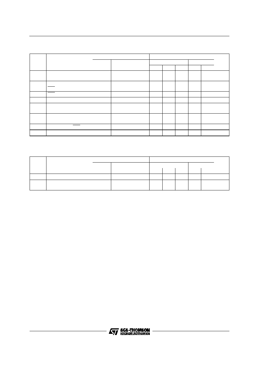
TEST CIRCUIT
C
L
= 50 pF or equivalent (includes jig and probe capacitance)
R
L
= R
1
= 500
or equivalent
R
T
= Z
OUT
of pulse generator (typically 50
)
WAVEFORM 1: PROPAGATION DELAYS, SETUP AND HOLD TIMES (f=1MHz; 50% duty cycle)
74ACT174
6/10
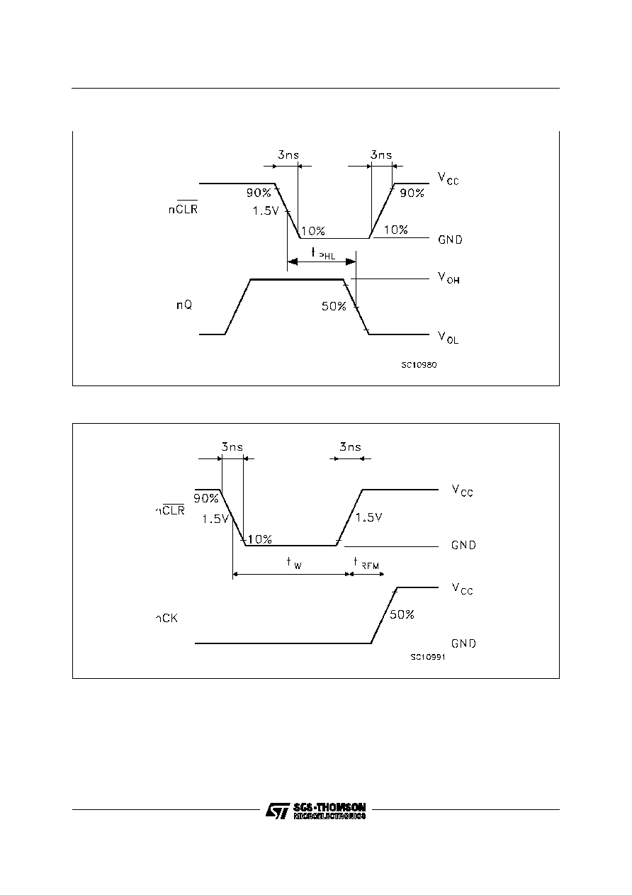
WAVEFORM 2: PROPAGATION DELAYS (f=1MHz; 50% duty cycle)
WAVEFORM 3: RECOVERY TIME (f=1MHz; 50% duty cycle)
74ACT174
7/10
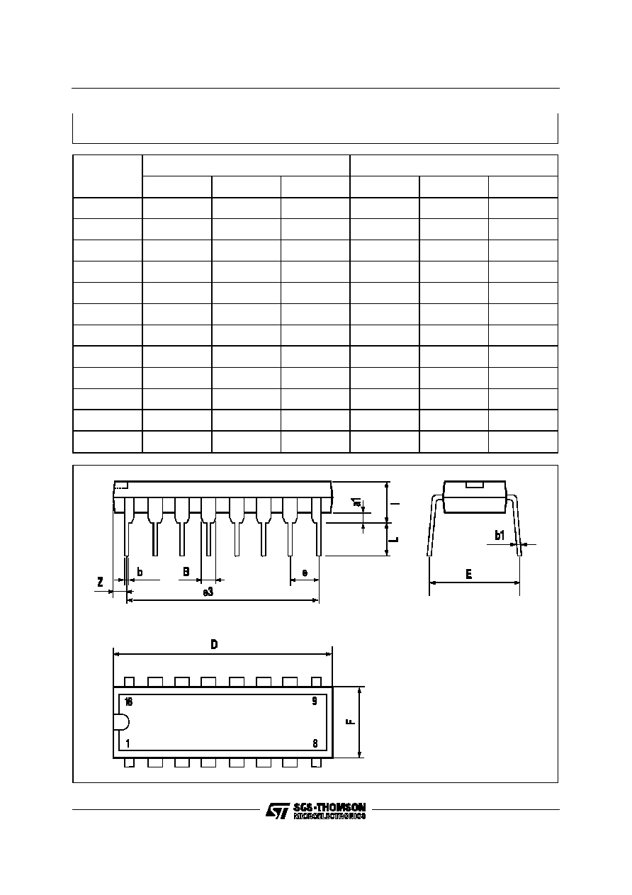
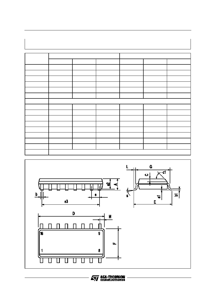
DIM.
mm
inch
MIN.
TYP.
MAX.
MIN.
TYP.
MAX.
a1
0.51
0.020
B
0.77
1.65
0.030
0.065
b
0.5
0.020
b1
0.25
0.010
D
20
0.787
E
8.5
0.335
e
2.54
0.100
e3
17.78
0.700
F
7.1
0.280
I
5.1
0.201
L
3.3
0.130
Z
1.27
0.050
P001C
Plastic DIP-16 (0.25) MECHANICAL DATA
74ACT174
8/10
DIM.
mm
inch
MIN.
TYP.
MAX.
MIN.
TYP.
MAX.
A
1.75
0.068
a1
0.1
0.2
0.004
0.007
a2
1.65
0.064
b
0.35
0.46
0.013
0.018
b1
0.19
0.25
0.007
0.010
C
0.5
0.019
c1
45 (typ.)
D
9.8
10
0.385
0.393
E
5.8
6.2
0.228
0.244
e
1.27
0.050
e3
8.89
0.350
F
3.8
4.0
0.149
0.157
G
4.6
5.3
0.181
0.208
L
0.5
1.27
0.019
0.050
M
0.62
0.024
S
8 (max.)
P013H
SO-16 MECHANICAL DATA
74ACT174
9/10

Information furnished is believed to be accurate and reliable. However, SGS-THOMSON Microelectronics assumes no responsability for the
consequences of use of such information nor for any infringement of patents or other rights of third parties which may results from its use. No
license is granted by implication or otherwise under any patent or patent rights of SGS-THOMSON Microelectronics. Specifications mentioned
in this publication are subject to change without notice. This publication supersedes and replaces all information previously supplied.
SGS-THOMSON Microelectronics products are not authorized for use as critical components in life support devices or systems without express
written approval of SGS-THOMSON Microelectonics.
©
1997 SGS-THOMSON Microelectronics - Printed in Italy - All Rights Reserved
SGS-THOMSON Microelectronics GROUP OF COMPANIES
Australia - Brazil - Canada - China - France - Germany - Hong Kong - Italy - Japan - Korea - Malaysia - Malta - Morocco - The Netherlands -
Singapore - Spain - Sweden - Switzerland - Taiwan - Thailand - United Kingdom - U.S.A
.
74ACT174
10/10