
1/9
July 2003
s
HIGH SPEED: t
PD
= 4.8ns (TYP.) at V
CC
= 5V
s
LOW POWER DISSIPATION:
I
CC
= 8
µ
A(MAX.) at T
A
=25∞C
s
COMPATIBLE WITH TTL OUTPUTS
V
IH
= 2V (MIN.), V
IL
= 0.8V (MAX.)
s
SYMMETRICAL OUTPUT IMPEDANCE:
|I
OH
| = I
OL
= 24mA (MIN) at V
CC
= 4.5V
s
BALANCED PROPAGATION DELAYS:
t
PLH
t
PHL
s
OPERATING VOLTAGE RANGE:
V
CC
(OPR) = 4.5V to 5.5V
s
FUNCTION COMPATIBLE WITH SERIES
16373 AND 16245 (244)
s
IMPROVED LATCH-UP IMMUNITY
s
IMPROVED ESD IMMUNITY
DESCRIPTION
The 74ACT16244 is a low voltage CMOS 16-BIT
D-TYPE LATCH and 16 BIT BUS TRANSCEIVER
with 3-STATE output non inverting fabricated with
sub-micron silicon gate and double-layer metal
wiring C
2
MOS technology.
Both functions can be used as 16 bit or dual octal
devices, so the 16 bit transceiver can be used ad 8
bit bus buffer plus 8 bit transceiver, or only 16 bit
buffer in select direction.
This device can be used to integrate in one chip
the internal logic component required to STV0701
to work ad P.O.D. interface in
Digital TV
application. It is ideal for low power and high
speed 4.5 to 5.5. applications.
All
inputs
and
outputs
are
equipped
with
protection circuits against static discharge, giving
them ESD immunity and transient excess voltage.
74ACT32701
16-BIT D-TYPE LATCH PULS 16-BIT BUS BUFFER
WITH 3-STATE OUTPUTS (NON INVERTED)
This is preliminary information on a new product now in development are or undergoing evaluation. Details subject to change without notice.
ORDER CODES
PACKAGE
TRAY
T & R
LFBGA96
74ACT32701LB
74ACT32701LBR
LFBGA96
(Top and Bottom view)
PRELIMINARY DATA
LOGIC DIAGRAM
74ACT32701
2/9
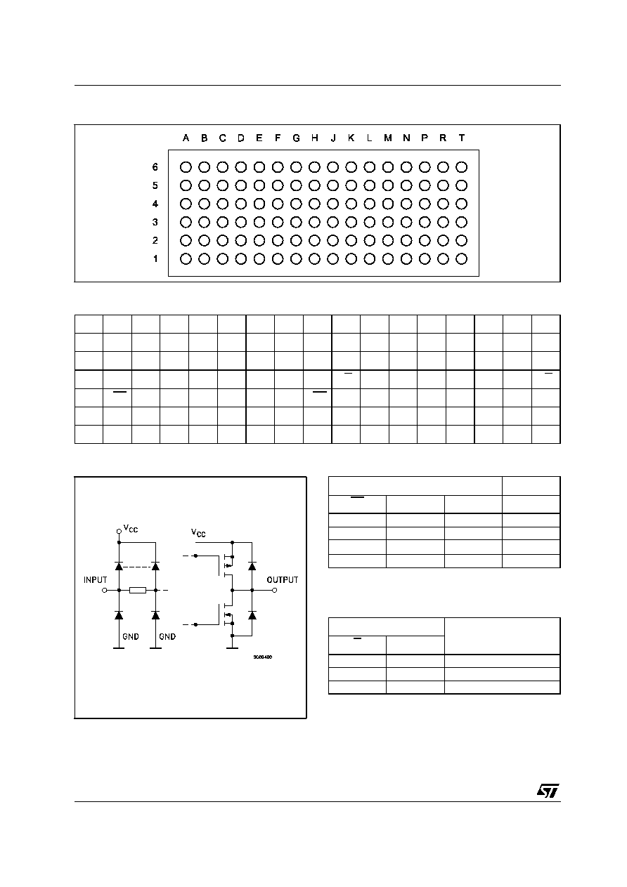
PIN CONNECTION (Top view)
TERMINAL ASSIGNMENT
INPUT AND OUTPUT EQUIVALENT CIRCUIT
TRUTH TABLE (each 8bit section of 16bit Latch)
TRUTH TABLE (each 8bit section of 16bit
Transceiver)
X : Don`t Care
Z : High Impedance
A
B
C
D
E
F
G
H
J
K
L
M
N
P
R
T
6
1D2
1D4
1D6
1D8
2D2
2D4
2D6
2D7
3A2
3A4
3A6
3A8
4A2
4A4
4A6
4A7
5
1D1
1D3
1D5
1D7
2D1
2D3
2D5
2D8
3A1
3A3
3A5
3A7
4A1
4A3
4A5
4A8
4
1LE
GND
V
CC
GND GND
V
CC
GND
2LE
3G
GND
V
CC
GND GND
V
CC
GND
4G
3
1OE
GND
V
CC
GND GND
V
CC
GND
2OE
3DIR GND
V
CC
GND GND
V
CC
GND 4DIR
2
1Q1
1Q3
1Q5
1Q7
2Q1
2Q3
2Q5
2B8
3B1
3B3
3B5
3B7
4B1
4B3
4B5
4B8
1
1Q2
1Q4
1Q6
1Q8
2Q2
2Q4
2Q6
2B7
3B2
3B4
3B6
3B8
4B2
4B4
4B6
4B7
INPUTS
OUTPUT
OE
LE
D
Q
L
H
H
H
L
H
L
L
L
L
X
Q
0
H
X
X
Z
INPUTS
OPERATION
G
DIR
L
L
B data to A bus
L
H
A data to B bus
H
X
Isolation

74ACT32701
3/9
ABSOLUTE MAXIMUM RATINGS
Absolute Maximum Ratings are those values beyond which damage to the device may occur. Functional operation under these conditions is
not implied.
RECOMMENDED OPERATING CONDITIONS
1) V
IN
from 0.8V to 2.0V
Symbol
Parameter
Value
Unit
V
CC
Supply Voltage
-0.5 to +7
V
V
I
DC Input Voltage
-0.5 to V
CC
+ 0.5
V
V
O
DC Output Voltage
-0.5 to V
CC
+ 0.5
V
I
IK
DC Input Diode Current
±
20
mA
I
OK
DC Output Diode Current
±
20
mA
I
O
DC Output Current
±
50
mA
I
CC
or I
GND
DC V
CC
or Ground Current
±
400
mA
T
stg
Storage Temperature
-65 to +150
∞C
T
L
Lead Temperature (10 sec)
300
∞C
Symbol
Parameter
Value
Unit
V
CC
Supply Voltage
4.5 to 5.5
V
V
I
Input Voltage
0 to V
CC
V
V
O
Output Voltage
0 to V
CC
V
T
op
Operating Temperature
-40 to 85
∞C
dt/dv
Input Rise and Fall Time V
CC
= 4.5 to 5.5V (note 1)
8
ns/V

74ACT32701
4/9
DC SPECIFICATIONS
1) Maximum test duration 2ms, one output loaded at time
2) Incident wave switching is guaranteed on transmission lines with impedances as low as 50
AC ELECTRICAL CHARACTERISTICS (C
L
= 50 pF, R
L
= 500
, Input t
r
= t
f
= 3ns)
(*) Voltage range is 5.0V
±
0.5V
Symbol
Parameter
Test Condition
Value
Unit
V
CC
(V)
T
A
= 25∞C
-40 to 85∞C
Min.
Typ.
Max.
Min.
Max.
V
IH
High Level Input Voltage
4.5
V
O
= 0.1 V or V
CC
-0.1V
2.0
2.0
V
5.5
2.0
2.0
V
IL
Low Level Input Voltage
4.5
V
O
= 0.1 V or V
CC
-0.1V
0.8
0.8
5.5
0.8
0.8
V
V
OH
High Level Output Voltage
4.5
I
O
=-50
µ
A
4.4
4.49
4.4
5.5
I
O
=-50
µ
A
5.4
5.49
5.4
4.5
I
O
=-24 mA
3.86
3.76
V
5.5
I
O
=-24 mA
4.86
4.76
V
OL
Low Level Output Voltage
4.5
I
O
=50
µ
A
0.001
0.1
0.1
5.5
I
O
=50
µ
A
0.001
0.1
0.1
4.5
I
O
=24 mA
0.36
0.44
5.5
I
O
=24 mA
0.36
0.44
I
I
Input Leakage Current
5.5
V
I
= V
CC
or GND
±
0.1
±
1
µ
A
I
OZ
High Impedance Output
Leakage Current
5.5
V
I
= V
IH
or V
IIL
V
O
=
V
CC
or GND
±
0.5
±
5
µ
A
I
CCT
Max I
CC
/Input
5.5
V
I
= V
CC
- 2.1V
0.9
1
mA
I
CC
Quiescent Supply Current
5.5
V
I
= V
CC
or GND
8
80
µ
A
I
OLD
Dynamic Output Current
(note 1, 2)
5.5
V
OLD
= 1.65 V max
75
mA
I
OHD
V
OHD
= 3.85 V min.
-75
mA
Symbol
Parameter
Test Condition
Value
Unit
V
CC
(V)
T
A
= 25∞C
-40 to 85∞C
Min.
Typ.
Max.
Min.
Max.
t
PLH
Propagation Delay Time
5.0
(*)
2.0
3.3
5.0
2.0
6.0
ns
t
PHL
3.0
4.8
6.5
3.0
8.0
t
PZL
Output Enable Time
5.0
(*)
4.0
6.5
8.7
4.0
9.7
ns
t
PZH
3.0
5.5
7.7
3.0
8.8
t
PLZ
Output Disable Time
5.0
(*)
4.0
6.0
8.0
4.0
9.2
ns
t
PHZ
3.0
4.6
6.4
3.0
7.3
74ACT32701
5/9
CAPACITIVE CHARACTERISTICS
1) C
PD
is defined as the value of the IC's internal equivalent capacitance which is calculated from the operating current consumption without
load. (Refer to Test Circuit). Average operating current can be obtained by the following equation. I
CC(opr)
= C
PD
x V
CC
x f
IN
+ I
CC
/n (per circuit)
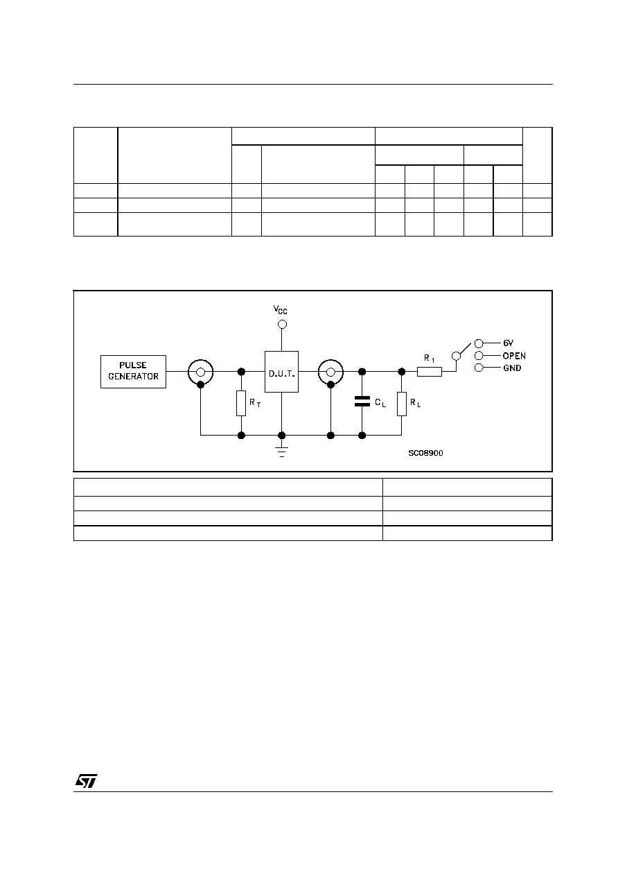
TEST CIRCUIT
C
L
= 50pF or equivalent (includes jig and probe capacitance)
R
L
= R
1
= 500
or equivalent
R
T
= Z
OUT
of pulse generator (typically 50
)
Symbol
Parameter
Test Condition
Value
Unit
V
CC
(V)
T
A
= 25∞C
-40 to 85∞C
Min.
Typ.
Max.
Min.
Max.
C
IN
Input Capacitance
5.0
3.6
pF
C
OUT
Output Capacitance
5.0
11
pF
C
PD
Power Dissipation Capaci-
tance (note 1)
5.0
f
IN
= 10MHz
42
pF
Test
Switch
t
PLH,
t
PHL
Open
t
PZL,
t
PLZ
2V
CC
t
PZH,
t
PHZ
GND