74ACT541
OCTAL BUS BUFFER
WITH 3 STATE OUTPUTS (NON INVERTED)
Æ
December 1998
s
HIGH SPEED: t
PD
= 4 ns (TYP.) at V
CC
= 5V
s
LOW POWER DISSIPATION:
I
CC
= 8
µ
A (MAX.) at T
A
= 25
o
C
s
COMPATIBLE WITH TTL OUTPUTS
V
IH
= 2V (MIN), V
IL
= 0.8V (MAX)
s
50
TRANSMISSION LINE DRIVING
CAPABILITY
s
SYMMETRICAL OUTPUT IMPEDANCE:
|I
OH
| = I
OL
= 24 mA (MIN)
s
BALANCED PROPAGATION DELAYS:
t
PLH
t
PHL
s
OPERATING VOLTAGE RANGE:
V
CC
(OPR) = 4.5V to 5.5V
s
PIN AND FUNCTION COMPATIBLE WITH
74 SERIES 541
s
IMPROVED LATCH-UP IMMUNITY
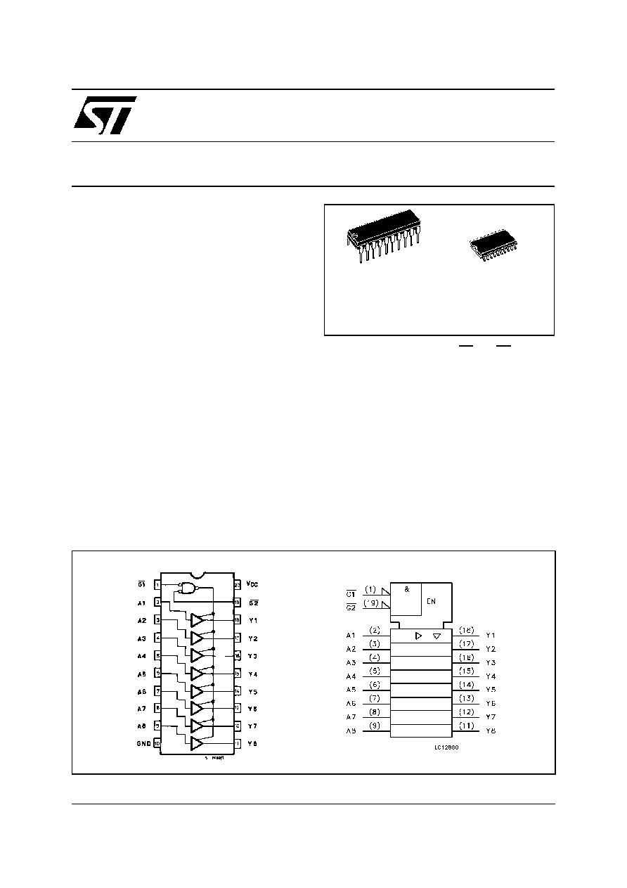
DESCRIPTION
The ACT541 is an advanced CMOS OCTAL BUS
BUFFER (3-STATE) fabricated with sub-micron
silicon gate and double-layer metal wiring C
2
MOS
technology.It is ideal for low power applications
mantaining high speed operation similar to
eqivalent Bipolar Schottky TTL.
The 3 STATE control gate operates as a two
input AND such that if either G1 and G2 are high,
all eight outputs are in the high impedance state.
In order to enhance PC board layout, the AC541
offers a pinout having inputs and outputs on
opposite sides of the package.
The device is designed to interface directly High
Speed CMOS systems with TTL, NMOS and
CMOS output voltage levels.
All inputs
and
outputs are
equipped with
protection circuits against static discharge, giving
them 2KV ESD immunity and transient excess
voltage.
PIN CONNECTION AND IEC LOGIC SYMBOLS
ORDER CODES :
74ACT541B
74ACT541M
M
(Micro Package)
B
(Plastic Package)
1/8
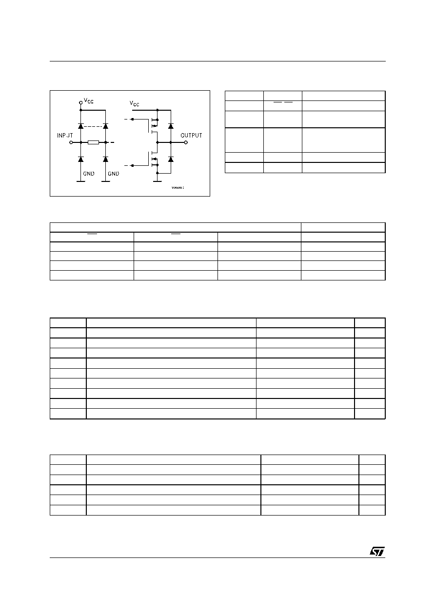
INPUT AND OUTPUT EQUIVALENT CIRCUIT
TRUTH TABLE
INPUT
O UT PUT
G 1
G 2
An
Yn
H
X
X
Z
X
H
X
Z
L
L
H
H
L
L
L
L
X:"H" or "L"
Z: High impedance
PIN DESCRIPTION
PIN No
SYMBOL
NAME AND FUNCT ION
1,19
G1, G2
Output Enable Input
2, 3, 4,5,
6, 7,8, 9
A1 to A8
Data Inputs
18, 17, 16,
15, 14, 13,
12, 11
Y1 to Y8
Data Outputs
10
GND
Ground (0V)
20
V
CC
Positive Supply Voltage
ABSOLUTE MAXIMUM RATINGS
Symbol
Parameter
Val ue
Unit
V
CC
Supply Voltage
-0.5 to +7
V
V
I
DC Input Voltage
-0.5 to V
CC
+ 0.5
V
V
O
DC Output Voltage
-0.5 to V
CC
+ 0.5
V
I
IK
DC Input Diode Current
±
20
mA
I
OK
DC Output Diode Current
±
20
mA
I
O
DC Output Current
±
50
mA
I
CC
orI
GND
DC V
CC
or Ground Current
±
400
mA
T
stg
Storage Temperature
-65 to +150
o
C
T
L
Lead Temperature (10 sec)
300
o
C
Absolute Maximum Ratings are those values beyond which damage to the device may occur. Functional operation under these condition is not implied.
RECOMMENDED OPERATING CONDITIONS
Symbol
Parameter
Value
Unit
V
CC
Supply Voltage
4.5 to 5.5
V
V
I
Input Voltage
0 to V
CC
V
V
O
Output Voltage
0 to V
CC
V
T
op
Operating Temperature:
-40 to +85
o
C
dt/dv
Input Rise and Fall Time V
CC
= 4.5 to 5.5V (note 1)
8
ns/V
1) V
IN
from 0.8 V to 2.0 V
74ACT541
2/8
DC SPECIFICATIONS
Symb ol
Parameter
Test Co nditi ons
Valu e
Un it
V
CC
(V)
T
A
= 25
o
C
-40 to 85
o
C
Min.
T yp.
Max.
Mi n.
Max.
V
IH
High Level Input Voltage
4.5
V
O
= 0.1 V or
V
CC
- 0.1 V
2.0
1.5
2.0
V
5.5
2.0
1.5
2.0
V
IL
Low Level Input Voltage
4.5
V
O
= 0.1 V or
V
CC
- 0.1 V
1.5
0.8
0.8
V
5.5
1.5
0.8
0.8
V
OH
High Level Output
Voltage
4.5
V
I
(*)
=
V
IH
or
V
IL
I
O
=-50
µ
A
4.4
4.49
4.4
V
5.5
I
O
=-50
µ
A
5.4
5.49
5.4
4.5
I
O
=-24 mA
3.86
3.76
5.5
I
O
=-24 mA
4.86
4.76
V
OL
Low Level Output
Voltage
4.5
V
I
(*)
=
V
IH
or
V
IL
I
O
=50
µ
A
0.001
0.1
0.1
V
5.5
I
O
=50 mA
0.001
0.1
0.1
4.5
I
O
=24 mA
0.36
0.44
5.5
I
O
=24 mA
0.36
0.44
I
I
Input Leakage Current
5.5
V
I
= V
CC
orGND
±
0.1
±
1
µ
A
I
OZ
3 State Output Leakage
Current
5.5
V
I
= V
IH
orV
IL
V
O
= V
CC
orGND
±
0.5
±
5
µ
A
I
CCT
Max I
CC
/Input
5.5
V
I
= V
CC
-2.1V
0.6
1.5
mA
I
CC
Quiescent Supply
Current
5.5
V
I
= V
CC
orGND
4
40
µ
A
I
OLD
Dynamic Output Current
(note 1, 2)
5.5
V
OLD
= 1.65 V max
75
mA
I
OHD
V
OHD
= 3.85 V min
-75
mA
1) Maximum test duration 2ms, one output loaded attime
2) Incident wave switching is guaranteed on transmission lines with impedances as low as 50
.
CAPACITIVE CHARACTERISTICS
Symbo l
Parameter
Test Con dition s
Value
Uni t
V
CC
(V)
T
A
= 25
o
C
-40 to 85
o
C
Mi n.
T yp.
Max.
Min.
Max.
C
IN
Input Capacitance
5.0
4
pF
C
PD
Power Dissipation
Capacitance (note 1)
5.0
22
pF
1) C
PD
is defined as the value of the IC's internal equivalent capacitance which is calculated from the operating current consumption without load. (Refer to
Test Circuit). Average operating current can be obtained by the following equation. I
CC
(opr) = C
PD
∑
V
CC
∑
f
IN
+ I
CC
/8 (per circuit)
AC ELECTRICAL CHARACTERISTICS (C
L
= 50 pF, R
L
= 500
, Input t
r
= t
f
=3 ns)
Symb ol
Parameter
T est Con ditio n
Valu e
Un it
V
CC
(V)
T
A
= 25
o
C
-40 to 85
o
C
Min.
T yp.
Max.
Mi n.
Max.
t
PLH
t
PHL
Propagation Delay Time
5.0
(*)
1.5
5
6.5
1.5
7.15
ns
t
PZL
t
PZH
Output Enable Time
5.0
(*)
1.5
6
7.8
1.5
8.5
ns
t
PLZ
t
PHZ
Output Disable Time
5.0
(*)
1.5
6
7.8
1.5
8.5
ns
(*) Voltage range is 5V
±
0.5V
74ACT541
3/8
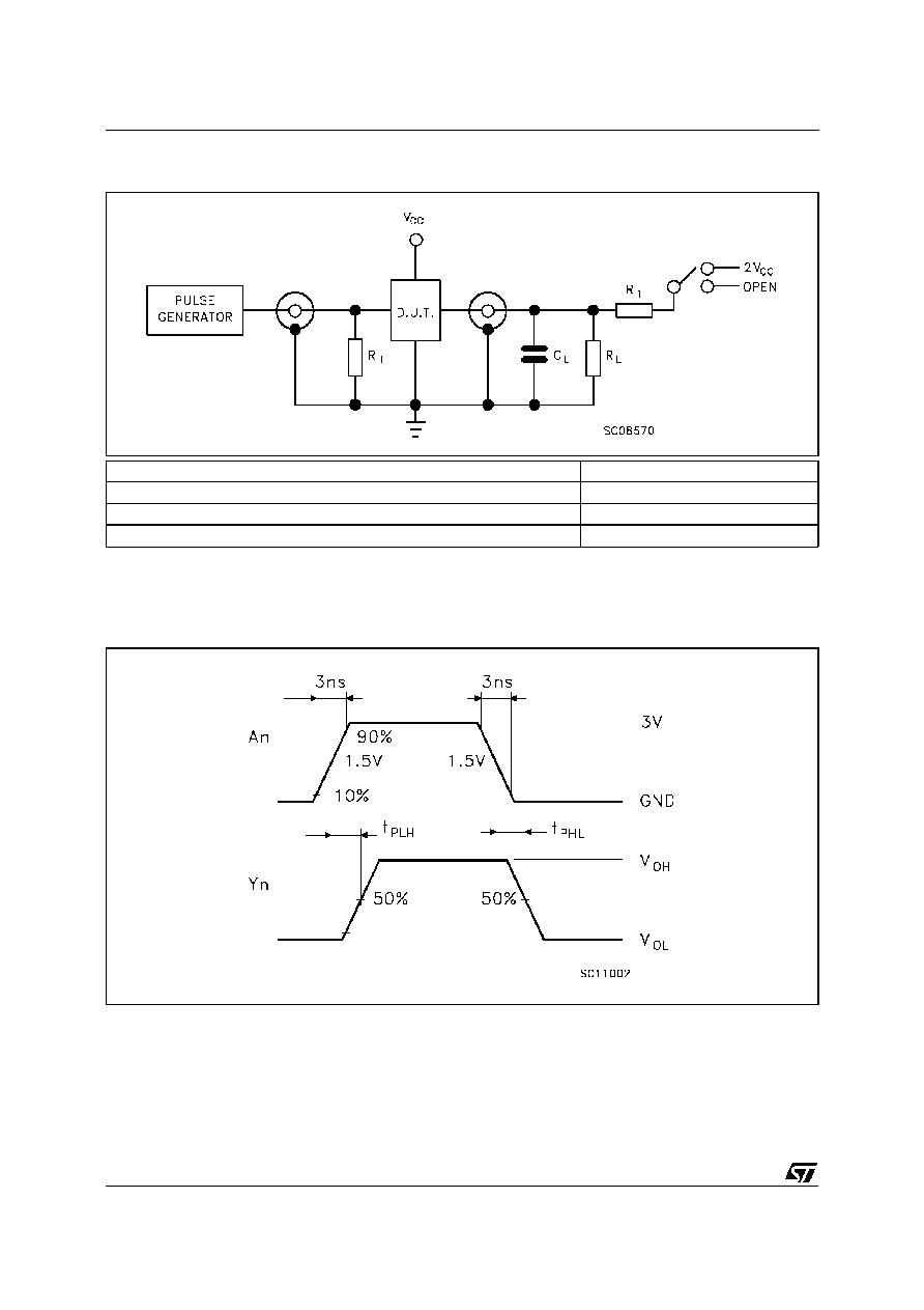
TEST CIRCUIT
T EST
SW IT CH
t
PLH
, t
PHL
Open
t
PZL
, t
PLZ
2V
CC
t
PZH
, t
PHZ
Open
C
L
= 50 pF or equivalent (includes jigand probe capacitance)
R
L
= R
1
= 500
orequivalent
R
T
= Z
OUT
of pulse generator (typically 50
)
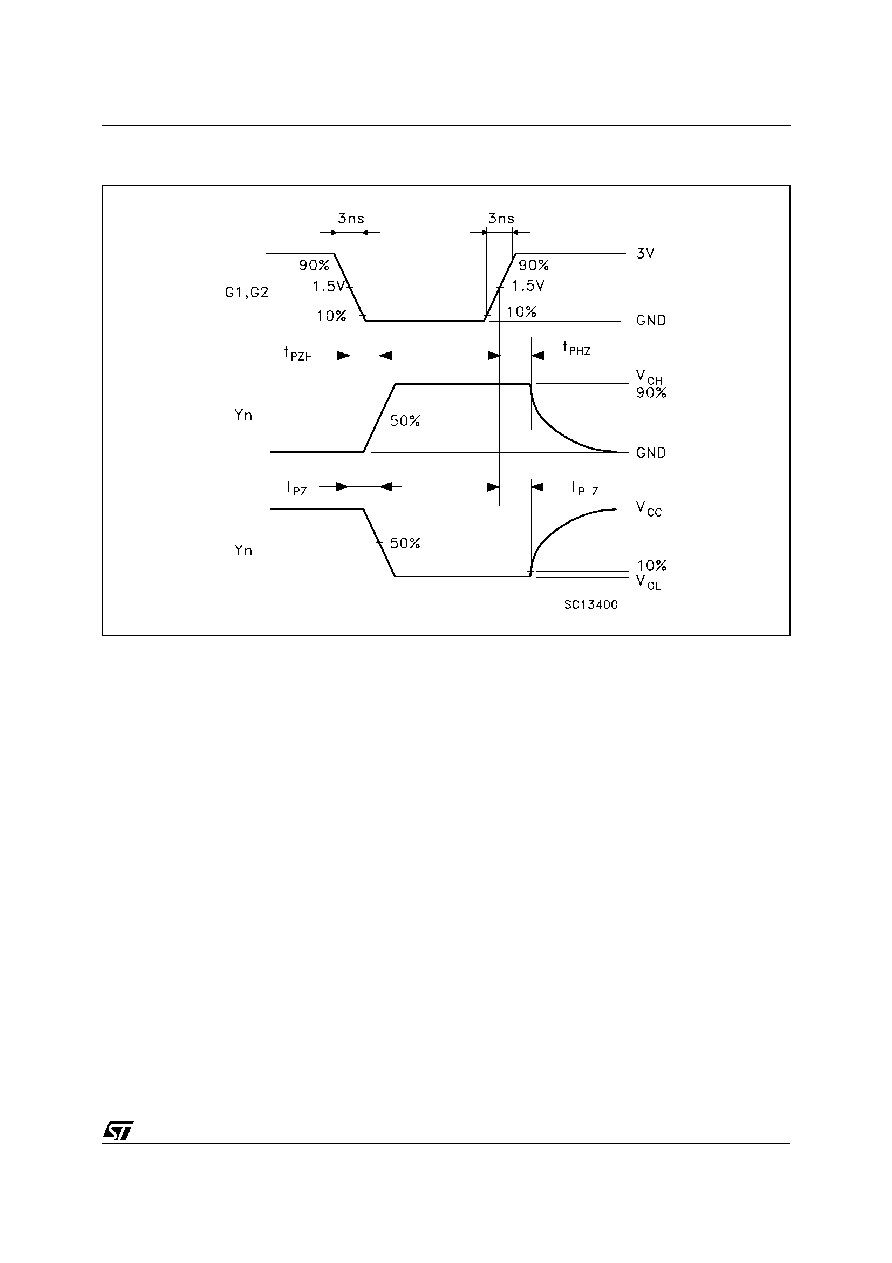
WAVEFORM 1: PROPAGATION DELAYS (f=1MHz; 50% duty cycle)
74ACT541
4/8