
1/10
July 2003
s
3.6V TOLERANT INPUTS AND OUTPUTS
s
HIGH SPEED:
t
PD
= 3.0 ns (MAX.) at V
CC
= 3.0 to 3.6V
t
PD
= 3.7 ns (MAX.) at V
CC
= 2.3 to 2.7V
t
PD
=6 ns (MAX.) at V
CC
= 1.65V
s
POWER DOWN PROTECTION ON INPUTS
AND OUTPUTS
s
SYMMETRICAL OUTPUT IMPEDANCE:
|I
OH
| = I
OL
= 24mA (MIN) at V
CC
= 3.0V
|I
OH
| = I
OL
= 12mA (MIN) at V
CC
= 2.3V
|I
OH
| = I
OL
= 4mA (MIN) at V
CC
= 1.65V
s
OPERATING VOLTAGE RANGE:
V
CC
(OPR) = 1.65V to 3.6V
s
BUS HOLD PROVIDED ON DATA INPUTS
s
PIN AND FUNCTION COMPATIBLE WITH
74 SERIES 16245
s
LATCH-UP PERFORMANCE EXCEEDS
300mA (JESD 17)
s
ESD PERFORMANCE:
HBM > 2000V (MIL STD 883 method 3015);
MM > 200V
DESCRIPTION
The 74ALVCH16245 is a low voltage CMOS 16
BIT
BUS
TRANSCEIVER
fabricated
with
sub-micron silicon gate and five-layer metal wiring
C
2
MOS technology. It is ideal for low power and
very high speed 1.65 to 3.6V applications; it can
be interfaced to 3.6V signal environment for both
inputs and outputs.
This IC is intended for two-way asynchronous
communication
between
data
busses;
the
direction of data transmission is determined by
DIR input. The enable input G can be used to
disable the device so that the busses are
effectively isolated.
Bus hold on data inputs is provided in order to
eliminate
the
need
for
external
pull-up
or
pull-down resistor.
All
inputs
and
outputs
are
equipped
with
protection circuits against static discharge, giving
them 2KV ESD immunity and transient excess
voltage.
74ALVCH16245
LOW VOLTAGE CMOS 16-BIT TRANSCEIVER (3-STATE)
WITH 3.6V TOLERANT INPUTS AND OUTPUTS
ORDER CODES
PACKAGE
TUBE
T & R
TSSOP
74ALVCH16245TTR
TSSOP
PIN CONNECTION

74ALVCH16245
2/10
INPUT AND OUTPUT EQUIVALENT CIRCUIT
PIN DESCRIPTION
TRUTH TABLE
Z : High Impedance
X : Don`t Care
IEC LOGIC SYMBOLS
PIN No
SYMBOL
NAME AND FUNCTION
1
1DIR
Directional Control
2, 3, 5, 6, 8, 9,
11, 12
1B1 to 1B8 Data Inputs/Outputs
13, 14, 16, 17,
19, 20, 22, 23
2B1 to 2B8 Data Inputs/Outputs
24
2DIR
Directional Control
25
2G
Output Enable Input
36, 35, 33, 32,
30, 29, 27, 26
2A1 to 2A8 Data Inputs/Outputs
47, 46, 44, 43,
41, 40, 38, 38
1A1 to 1A8 Data Inputs/Outputs
48
1G
Output Enable Input
4, 10, 15, 21,
28, 34, 39, 45
GND
Ground (0V)
7, 18, 31, 42
V
CC
Positive Supply Voltage
INPUTS
FUNCTION
OUTPUT
G
DIR
A BUS
B BUS
Yn
L
L
OUTPUT
INPUT
A = B
L
H
INPUT
OUTPUT
B = A
H
X
Z
Z
Z
74ALVCH16245
3/10
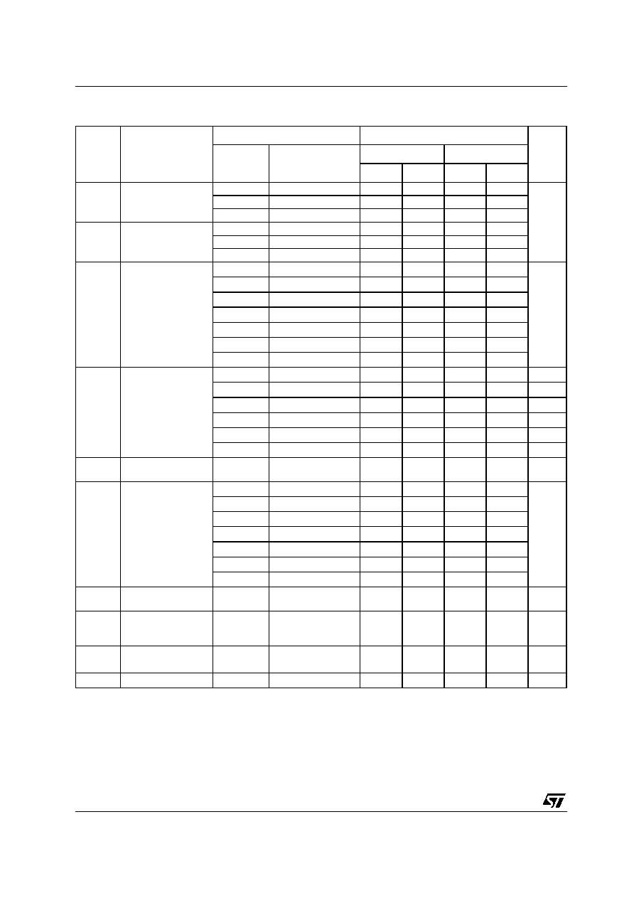
ABSOLUTE MAXIMUM RATINGS
Absolute Maximum Ratings are those values beyond which damage to the device may occur. Functional operation under these conditions is
not implied
1) I
O
absolute maximum rating must be observed
2) V
O
< GND, V
O
> V
CC
RECOMMENDED OPERATING CONDITIONS
1) V
IN
from 0.8V to 2V at V
CC
= 3.0V
Symbol
Parameter
Value
Unit
V
CC
Supply Voltage
-0.5 to +4.6
V
V
I
DC Input Voltage
-0.5 to +4.6
V
V
O
DC Output Voltage (OFF State)
-0.5 to +4.6
V
V
O
DC Output Voltage (High or Low State) (note 1)
-0.5 to V
CC
+ 0.5
V
I
IK
DC Input Diode Current
- 50
mA
I
OK
DC Output Diode Current (note 2)
- 50
mA
I
O
DC Output Current
�
50
mA
I
CC
or I
GND
DC V
CC
or Ground Current per Supply Pin
�
100
mA
P
D
Power Dissipation
400
mW
T
stg
Storage Temperature
-65 to +150
�C
T
L
Lead Temperature (10 sec)
300
�C
Symbol
Parameter
Value
Unit
V
CC
Supply Voltage
1.65 to 3.6
V
V
I
Input Voltage
-0.3 to 3.6
V
V
O
Output Voltage (OFF State)
0 to 3.6
V
V
O
Output Voltage (High or Low State)
0 to V
CC
V
I
OH
, I
OL
High or Low Level Output Current (V
CC
= 3.0 to 3.6V)
�
24
mA
I
OH
, I
OL
High or Low Level Output Current (V
CC
= 2.3 to 2.7V)
�
12
mA
I
OH
, I
OL
High or Low Level Output Current (V
CC
= 1.65V)
�
4
mA
T
op
Operating Temperature
-55 to 125
�C
dt/dv
Input Rise and Fall Time (note 1)
0 to 10
ns/V
74ALVCH16245
4/10
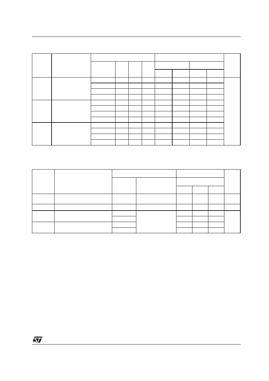
DC SPECIFICATIONS
Symbol
Parameter
Test Condition
Value
Unit
V
CC
(V)
-40 to 85 �C
-55 to 125 �C
Min.
Max.
Min.
Max.
V
IH
High Level Input
Voltage
1.65 to 1.95
0.65 Vcc
0.65 Vcc
V
2.3 to 2.7
1.7
1.7
2.7 to 3.6
2.0
2.0
V
IL
Low Level Input
Voltage
1.65 to 1.95
0.35 Vcc
0.35 Vcc
2.3 to 2.7
0.7
0.7
2.7 to 3.6
0.8
0.8
V
OH
High Level Output
Voltage
1.65 to 3.6
I
O
=-100
�
A
V
CC
-0.2
V
CC
-0.2
V
1.65
I
O
=-4 mA
1.2
1.2
2.3
I
O
=-6 mA
2.0
2.0
2.3
I
O
=-12 mA
1.7
1.7
2.7
I
O
=-12 mA
2.2
2.2
3.0
I
O
=-12 mA
2.4
2.4
3.0
I
O
=-24 mA
2.0
2.0
V
OL
Low Level Output
Voltage
1.65 to 3.6
I
O
=100
�
A
0.2
0.2
V
1.65
I
O
=4 mA
0.45
0.45
2.3
I
O
=6 mA
0.4
0.4
2.3
I
O
=12 mA
0.7
0.7
2.7
I
O
=12 mA
0.4
0.4
3.0
I
O
=24 mA
0.55
0.55
I
I
Input Leakage
Current
3.6
V
I
= 0 or 3.6V
�
5
�
5
�
A
I
IHOLD
Input Hold Current
1.65
V
I
=0.58 V
+ 25
+ 25
�
A
1.65
V
I
=1.07 V
- 25
- 25
2.3
V
I
=0.7 V
+ 45
+ 45
2.3
V
I
=1.7 V
- 45
- 45
3.0
V
I
=0.8 V
+ 75
+ 75
3.0
V
I
=2 V
- 75
- 75
3.6
V
I
= 0 to 3.6V
�
500
�
500
I
off
Power Off Leakage
Current
0
V
I
or V
O
= 3.6V
10
20
�
A
I
OZ
High Impedance
Output Leakage
Current
3.6
V
I
= V
IH
or V
IL
V
O
= 0 to V
CC
�
5
�
10
�
A
I
CC
Quiescent Supply
Current
3.6
V
I
= V
CC
or GND
I
O
= 0
20
40
�
A
I
CC
I
CC
incr. per Input
3.0 to 3.6
V
IH
= V
CC
- 0.6V
500
750
�
A
74ALVCH16245
5/10
AC ELECTRICAL CHARACTERISTICS
1) Skew is defined as the absolute value of the difference between the actual propagation delay for any two outputs of the same device switch-
ing in the same direction, either HIGH or LOW (t
OSLH
= | t
PLHm
- t
PLHn
|, t
OSHL
= | t
PHLm
- t
PHLn
|)
2) Parameter guaranteed by design
CAPACITIVE CHARACTERISTICS
1) C
PD
is defined as the value of the IC's internal equivalent capacitance which is calculated from the operating current consumption without
load. (Refer to Test Circuit). Average operating current can be obtained by the following equation. I
CC(opr)
= C
PD
x V
CC
x f
IN
+ I
CC
/16 (per
circuit)
Symbol
Parameter
Test Condition
Value
Unit
V
CC
(V)
C
L
(pF)
R
L
(
)
t
s
= t
r
(ns)
-40 to 85 �C
-55 to 125 �C
Min.
Max.
Min.
Max.
t
PLH
t
PHL
Propagation Delay
Time
1.65 to 1.95
30
1000
2.0
1
6
1
6
ns
2.3 to 2.7
30
500
2.0
1
3.7
1
3.7
2.7
50
500
2.5
1
3.6
1
3.6
3.0 to 3.6
50
500
2.5
1
3.0
1
3.0
t
PZL
t
PZH
Output Enable Time
1.65 to 1.95
30
1000
2.0
1
7.1
1
7.1
2.3 to 2.7
30
500
2.0
1
5.7
1
5.7
2.7
50
500
2.5
1
5.4
1
5.4
3.0 to 3.6
50
500
2.5
1
4.4
1
4.4
t
PLZ
t
PHZ
Output Disable Time
1.65 to 1.95
30
1000
2.0
1
7.0
1
7.0
2.3 to 2.7
30
500
2.0
1
5.2
1
5.2
2.7
50
500
2.5
1
4.6
1
4.6
3.0 to 3.6
50
500
2.5
1
4.1
1
4.1
Symbol
Parameter
Test Condition
Value
Unit
V
CC
(V)
T
A
= 25 �C
Min.
Typ.
Max.
C
IN
Input Capacitance Control
Inputs
3.3
V
IN
=V
CC
or GND
4
pF
C
I/O
Input Capacitance A or B ports
3.3
V
IN
=V
CC
or GND
8
pF
C
PD
Power Dissipation Capacitance
Output enabled (note 1)
3.3
f
IN
= 10MHz
C
L
=50pF
V
IN
= 0 or V
CC
29
pF
2.5
22
C
PD
Power Dissipation Capacitance
Output disabled (note 1)
3.3
5
2.5
4