1/10
July 2001
s
HIGH SPEED: t
PD
= 4ns (TYP.) at V
CC
= 4.5V
s
LOW POWER DISSIPATION:
I
CC
= 1
µ
A(MAX.) at T
A
=25∞C
s
HIGH NOISE IMMUNITY:
V
NIH
= V
NIL
= 28% V
CC
(MIN.)
s
LOW "ON" RESISTANCE:
R
ON
= 50
(TYP.) AT V
CC
= 9V I
I/O
= 100
µ
A
s
SINE WAVE DISTORTION:
0.042% AT V
CC
= 4V f = 1KHz
s
WIDE OPERATING RANGE:
V
CC
(OPR) = 2V TO 12V
DESCRIPTION
The 74H1G66 is a CMOS SINGLE BILATERAL
SWITCH fabricated in silicon gate C
2
MOS
technology. It achieves high speed performance
combined with true CMOS low power
consumption.
The C input is provided to control the switch and
it's compatible with standard CMOS output; the
switch is ON (port I/O is connected to Port O/I)
when the C input is held high and OFF (high
impedance state exists between the two ports)
when C is held low.
All inputs and output are equipped with protection
circuits against static discharge, giving them ESD
immunity and transient excess voltage.
74H1G66
SINGLE BILATERAL SWITCH
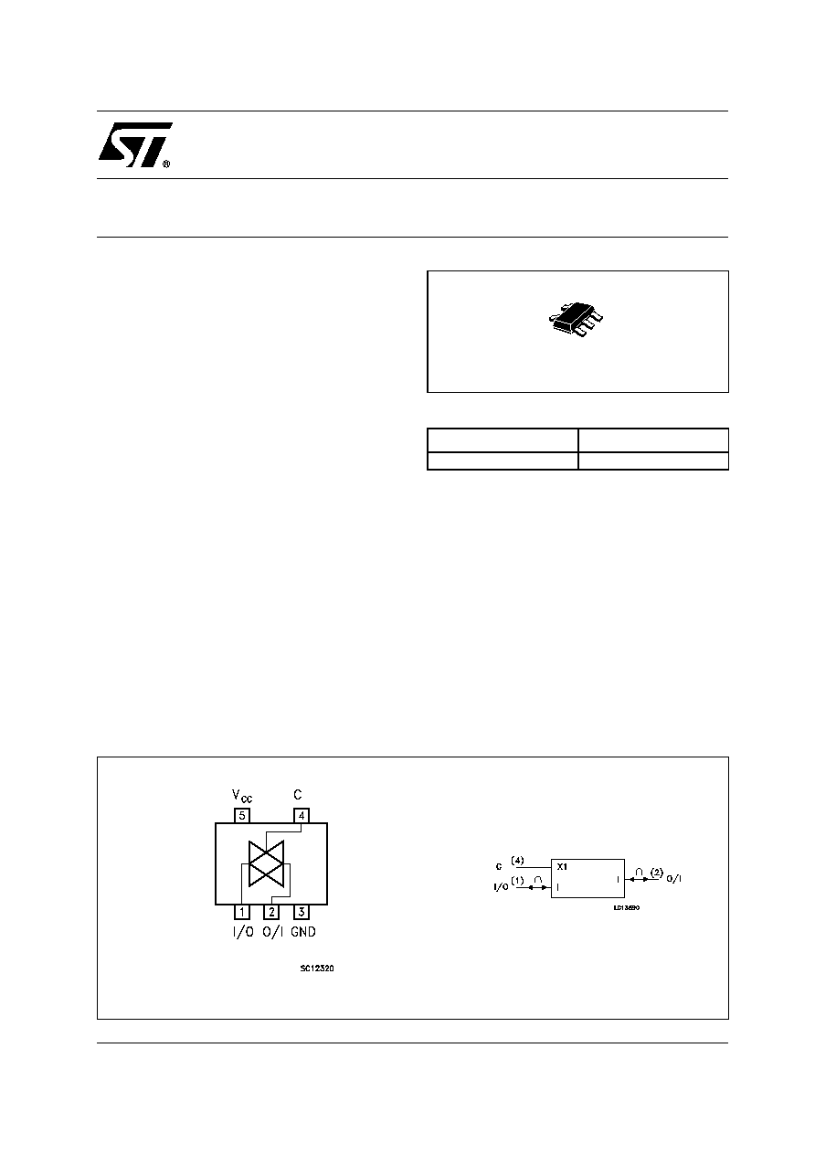
PIN CONNECTION AND IEC LOGIC SYMBOLS
ORDER CODES
PACKAGE
T & R
SOT23-5L
74H1G66STR
SOT23-5L

74H1G66
2/10
INPUT EQUIVALENT CIRCUIT
PIN DESCRIPTION
TRUTH TABLE
* High Impedance State
ABSOLUTE MAXIMUM RATINGS
Absolute Maximum Ratings are those values beyond which damage to the device may occur. Functional operation under these conditions is
not implied
(*) 500mW at 65
∞
C; derate to 300mW by 10mW/
∞
C from 65
∞
C to 85
∞
C
RECOMMENDED OPERATING CONDITIONS
PIN No
SYMBOL
NAME AND FUNCTION
1
I/O
Independent Input/Output
2
O/I
Independent Output/Input
3
GND
Ground (0V)
4
C
Enable Input (Active
HIGH)
5
V
CC
Positive Supply Voltage
C
SWITCH FUNCTION
H
ON
L
OFF *
Symbol
Parameter
Value
Unit
V
CC
Supply Voltage
-0.5 to +13.0
V
V
I/O
DC Input/Output Voltage
-0.5 to V
CC
+ 0.5
V
V
IC
DC Control Input Voltage
-0.5 to V
CC
+ 0.5
V
I
IOK
DC Input/Output Diode Current
±
20
mA
I
IK
DC Control Input Diode Current
±
20
mA
I
O
DC Output Source Sink Current per Output Pin
±
25
mA
I
CC
or I
GND
DC V
CC
or Ground Current
±
50
mA
P
D
Power Dissipation
500 (*)
mW
T
stg
Storage Temperature
-65 to +150
∞C
T
L
Lead Temperature (10 sec)
300
∞C
Symbol
Parameter
Value
Unit
V
CC
Supply Voltage
2 to 12
V
V
I
Control Input Voltage
0 to V
CC
V
V
I/O
Input/Output Voltage
0 to V
CC
V
T
op
Operating Temperature
-55 to 125
∞C
t
r
, t
f
Input Rise and Fall Time on control pin
V
CC
= 2.0V
0 to 1000
ns
V
CC
= 4.5V
0 to 500
ns
V
CC
= 6.0V
0 to 400
ns
V
CC
= 10.0V
0 to 250
ns
74H1G66
3/10
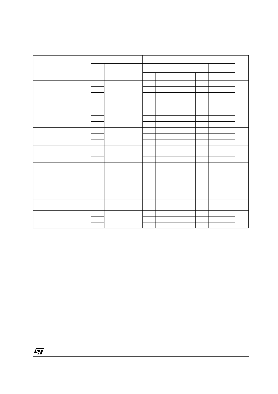
DC SPECIFICATIONS
Symbol
Parameter
Test Condition
Value
Unit
V
CC
(V)
T
A
= 25∞C
-40 to 85∞C
-55 to 125∞C
Min.
Typ.
Max.
Min.
Max.
Min.
Max.
V
IH
High Level Input
Voltage
2.0
1.5
1.5
1.5
V
4.5
3.15
3.15
3.15
9.0
6.3
6.3
6.3
12.0
8.4
8.4
8.4
V
IL
Low Level Input
Voltage
2.0
0.5
0.5
0.5
V
4.5
1.35
1.35
1.35
9.0
2.7
2.7
2.7
12.0
3.6
3.6
3.6
R
ON
ON Resistance
4.5
V
IC
= V
IH
V
I/O
= V
CC
to GND
I
I/O
1mA
96
170
200
250
9.0
55
85
100
150
12.0
45
80
90
120
R
ON
ON Resistance
4.5
V
IC
= V
IH
V
I/O
= V
CC
or GND
I
I/O
1mA
70
100
130
160
9.0
50
75
95
115
12.0
45
70
90
110
I
OFF
Input/Output
Leakage Current
(SWITCH OFF)
12.0
V
OS
= V
CC
to GND
V
IS
= V
CC
to GND
V
IC
= V
IL
±
0.1
±
1
±
2
µ
A
I
IZ
Switch Input
Leakage Current
(SWITCH ON,
OUTPUT OPEN)
12.0
V
OS
= V
CC
to GND
V
IC
= V
IH
±
0.1
±
1
±
2
µ
A
I
IN
Control Input
Leakage Current
6.0
V
IC
= 5.5V or GND
±
0.1
±
1.0
±
1.0
µ
A
I
CC
Quiescent Supply
Current
6.0
V
I
= V
CC
or GND
1
10
20
µ
A
9.0
4
40
80
12.0
8
80
160
74H1G66
4/10
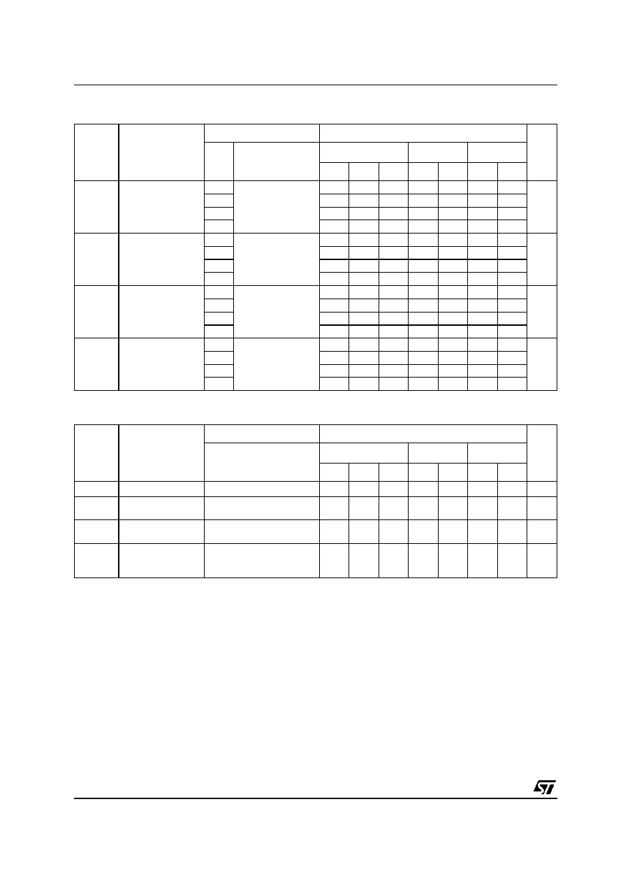
AC ELECTRICAL CHARACTERISTICS (C
L
= 50pF, Input t
r
= t
f
= 6ns)
CAPACITIVE CHARACTERISTICS
1) C
PD
is defined as the value of the IC's internal equivalent capacitance which is calculated from the operating current consumption without
load. (Refer to Test Circuit). Average operating current can be obtained by the following equation. I
CC(opr)
= C
PD
x V
CC
x f
IN
+ I
CC
Symbol
Parameter
Test Condition
Value
Unit
V
CC
(V)
T
A
= 25∞C
-40 to 85∞C
-55 to 125∞C
Min.
Typ.
Max.
Min.
Max.
Min.
Max.
I/O
Phase Difference
Between Input and
Output
2.0
10
50
65
75
ns
4.5
4
10
15
18
9.0
3
8
13
16
12.0
3
7
10
12
t
PLZ
t
PHZ
Output Disable
Time
2.0
R
L
= 500
18
100
125
150
ns
4.5
8
20
25
30
9.0
6
12
22
27
12.0
6
12
18
25
t
PZL
t
PZH
Output Enable
Time
2.0
R
L
= 1 K
20
115
145
175
ns
4.5
10
23
29
35
9.0
8
20
25
30
12.0
8
18
22
27
Maximum Control
Input Frequency
2.0
R
L
= 1 K
C
L
= 15pF
V
O
= 1/2V
CC
30
MHz
4.5
30
9.0
30
12.0
30
Symbol
Parameter
Test Condition
Value
Unit
T
A
= 25∞C
-40 to 85∞C
-55 to 125∞C
Min.
Typ.
Max.
Min.
Max.
Min.
Max.
C
IN
Input Capacitance
5
10
10
10
pF
C
I/O
Switch Terminal
Capacitance
10
pF
C
IOS
Feed through
Capacitance
0.5
pF
C
PD
Power Dissipation
Capacitance
(note 1)
15
pF
74H1G66
5/10
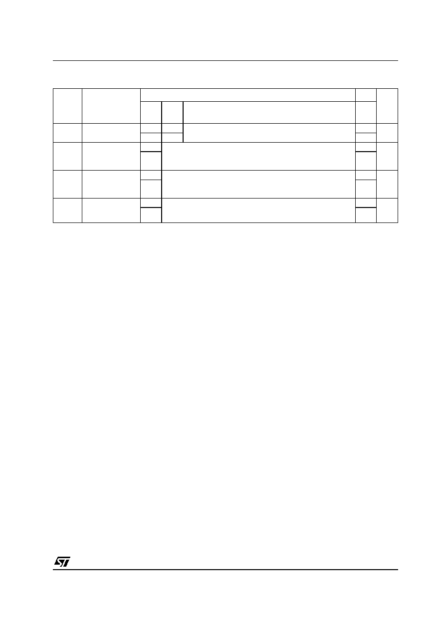
ANALOG SWITCH CHARACTERISTICS (GND = 0V; T
A
= 25∞C)
Symbol
Parameter
Test Condition
Value
Unit
V
CC
(V)
V
IN
(V
p-p
)
Typ.
Sine Wave
Distortion (THD)
4.5
4
f
IN
= 1 KHz R
L
= 10 K
, C
L
= 50 pF
0.04
%
9.0
8
0.04
f
MAX
Frequency
Response
(Switch ON)
4.5
Adjust f
IN
voltage to obtain 0 dBm at V
OS
.
Increase f
IN
Frequency until dB meter reads -3dB
R
L
= 50
, C
L
= 10 pF
150
MHz
9.0
180
Feed through
Attenuation
(Switch OFF)
4.5
V
IN
is centered at V
CC
/2
Adjust f
IN
Voltage to obtained 0dBm at V
IS
R
L
= 600
, C
L
= 50 pF, f
IN
= 1KHz sine wave
-60
dB
9.0
-60
Crosstalk (Control
Input to Signal
Output)
4.5
R
L
= 600
, C
L
= 50 pF, f
IN
= 1KHz square wave
t
r
= t
f
= 6ns
60
mV
9.0
60

74H1G66
6/10
SWITCHING CARACTERISTICS TEST CIRCUIT
CROSSTALK (control to output
BANDWIDTH AND FEEDTHROUGH ATTENUATION
MAXIMUM CONTROL FREQUENCY

74H1G66
7/10
CHANNEL RESISTANCE (R
ON)
I
CC
(Opr.)
74H1G66
8/10
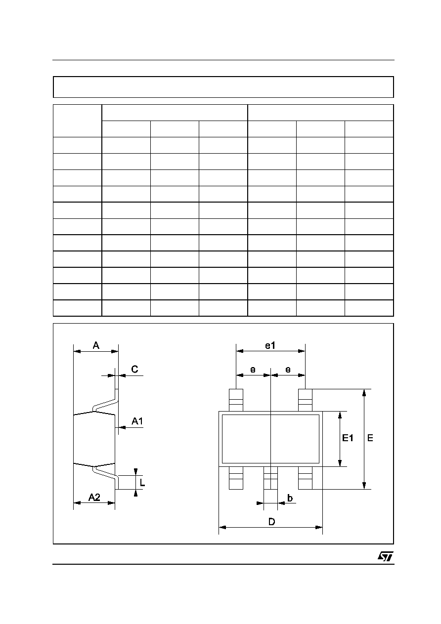
DIM.
mm.
mils
MIN.
TYP
MAX.
MIN.
TYP.
MAX.
A
0.90
1.45
35.4
57.1
A1
0.00
0.15
0.0
5.9
A2
0.90
1.30
35.4
51.2
b
0.35
0.50
13.7
19.7
C
0.09
0.20
3.5
7.8
D
2.80
3.00
110.2
118.1
E
2.60
3.00
102.3
118.1
E1
1.50
1.75
59.0
68.8
e
0.95
37.4
e1
1.9
74.8
L
0.35
0.55
13.7
21.6
SOT23-5L MECHANICAL DATA
74H1G66
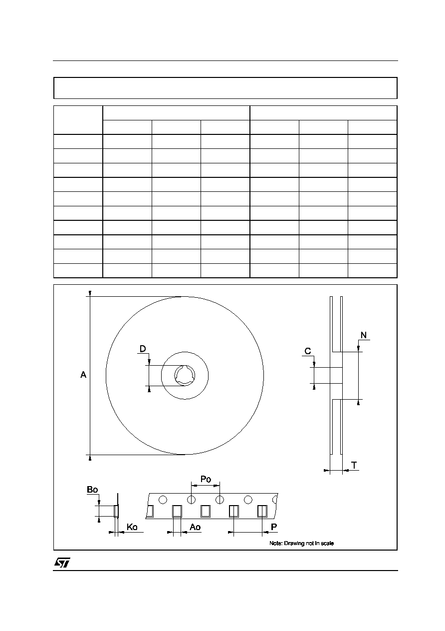
9/10
DIM.
mm.
inch
MIN.
TYP
MAX.
MIN.
TYP.
MAX.
A
180
7.086
C
12.8
13.0
13.2
0.504
0.512
0.519
D
20.2
0.795
N
60
2.362
T
14.4
0.567
Ao
3.13
3.23
3.33
0.123
0.127
0.131
Bo
3.07
3.17
3.27
0.120
0.124
0.128
Ko
1.27
1.37
1.47
0.050
0.054
0.0.58
Po
3.9
4.0
4.1
0.153
0.157
0.161
P
3.9
4.0
4.1
0.153
0.157
0.161
Tape & Reel SOT23-xL MECHANICAL DATA

74H1G66
10/10
Information furnished is believed to be accurate and reliable. However, STMicroelectronics assumes no responsibility for the
consequences of use of such information nor for any infringement of patents or other rights of third parties which may result from
its use. No license is granted by implication or otherwise under any patent or patent rights of STMicroelectronics. Specifications
mentioned in this publication are subject to change without notice. This publication supersedes and replaces all information
previously supplied. STMicroelectronics products are not authorized for use as critical components in life support devices or
systems without express written approval of STMicroelectronics.
© The ST logo is a registered trademark of STMicroelectronics
© 2001 STMicroelectronics - Printed in Italy - All Rights Reserved
STMicroelectronics GROUP OF COMPANIES
Australia - Brazil - China - Finland - France - Germany - Hong Kong - India - Italy - Japan - Malaysia - Malta - Morocco
Singapore - Spain - Sweden - Switzerland - United Kingdom
© http://www.st.com