M54HC155
M74HC155
December 1992
DUAL 2 TO 4 LINE DECODER 3 TO 8 LINE DECODER
B1R
(Plastic Package)
ORDER CODES :
M54HC155F1R
M74HC155M1R
M74HC155B1R
M74HC155C1R
F1R
(Ceramic Package)
M1R
(Micro Package)
C1R
(Chip Carrier)
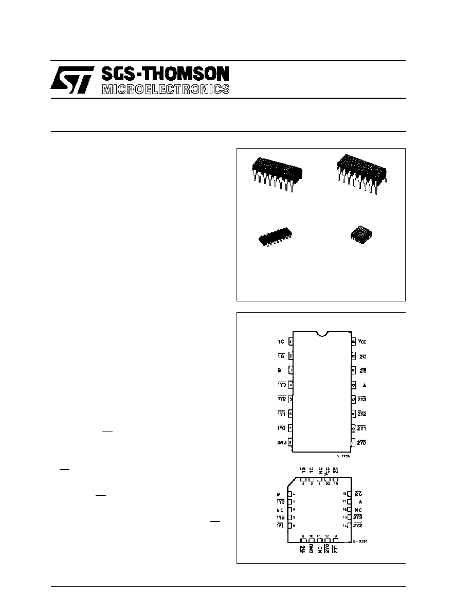
PIN CONNECTIONS (top view)
NC =
No Internal
Connection
DESCRIPTION
.
HIGH SPEED
t
PD
= 12 ns (TYP.) AT V
CC
= 5 V
.
LOW POWER DISSIPATION
I
CC
= 4
µ
A (MAX.) AT T
A
= 25
∞
C
.
HIGH NOISE IMMUNITY
V
NIH
= V
NIL
= 28 % V
CC
(MIN.)
.
OUTPUT DRIVE CAPABILITY
10 LSTTL LOADS
.
SYMMETRICAL OUTPUT IMPEDANCE
I
OH
= I
OL
= 4 mA (MIN.)
.
BALANCED PROPAGATION DELAYS
t
PLH
= t
PHL
.
WIDE OPERATING VOLTAGE RANGE
V
CC
(OPR) = 2 V TO 6 V
.
PIN AND FUNCTION COMPATIBLE
WITH 54/74LS155
The M54/74HC155 is a high speed CMOS DUAL 2-
TO-4 LINE DECODER fabricated in silicon gate
C
2
MOS technology.
It has the same high speed performance of LSTTL
combined with true CMOS low power consumption.
It features dual 1-TO-4 line demultiplexers with indi-
vidual strobe inputs (1G and 2G), individual data in-
puts (1C and 2C) and common binary address
inputs (A and B).
When both decoders are enabled by the strobes, the
inverted output of 1C data and non-inverted output
of 2C data will be brought to the select output pins
of each sections. A 1-TO-8 line demultiplexer can
also be easily built up by providing a data signal to
both 1C and 2C inputs ; the output order from the
msb is 1Y3, 1Y2, 1Y1, 1Y0, 2Y3, 2Y2, 2Y1, 2Y0.
This device can be used as a 2-to-4 line decoder or
a 3-to-8 line decoder when 1C is held high and 2C
is held low.
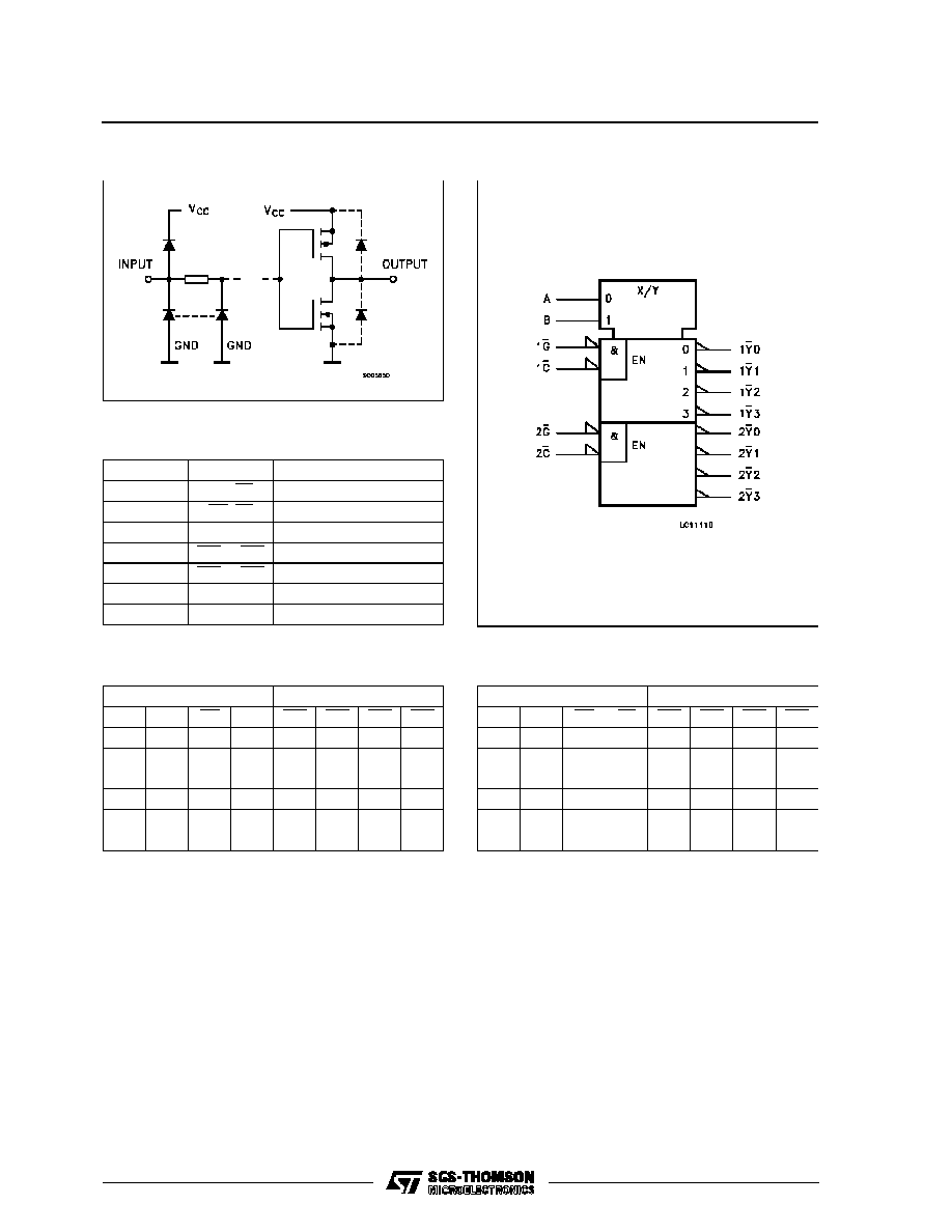
All inputs are equipped with protection circuits
against static discharge and transient excess volt-
age.
1/11
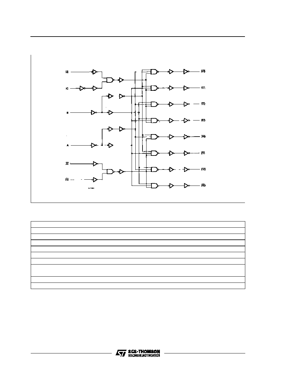
LOGIC CIRCUIT
ABSOLUTE MAXIMUM RATINGS
Symbol
Parameter
Value
Unit
V
CC
Supply Voltage
-0.5 to +7
V
V
I
DC Input Voltage
-0.5 to V
CC
+ 0.5
V
V
O
DC Output Voltage
-0.5 to V
CC
+ 0.5
V
I
IK
DC Input Diode Current
±
20
mA
I
OK
DC Output Diode Current
±
20
mA
I
O
DC Output Source Sink Current Per Output Pin
±
25
mA
I
CC
or I
GND
DC V
CC
or Ground Current
±
50
mA
P
D
Power Dissipation
500 (*)
mW
T
stg
Storage Temperature
-65 to +150
o
C
T
L
Lead Temperature (10 sec)
300
o
C
Absolute Maximum Ratings are those values beyond which damage to the device may occur. Functional operation under these condition is not implied.
(*) 500 mW:
65
o
C derate to 300 mW by 10mW/
o
C: 65
o
C to 85
o
C
M54/M74HC155
3/11
AC ELECTRICAL CHARACTERISTICS (C
L
= 50 pF, Input t
r
= t
f
= 6 ns)
Symbol
Parameter
Test Conditions
Value
Unit
V
CC
(V)
T
A
= 25
o
C
54HC and 74HC
-40 to 85
o
C
74HC
-55 to 125
o
C
54HC
Min.
Typ.
Max.
Min.
Max.
Min.
Max.
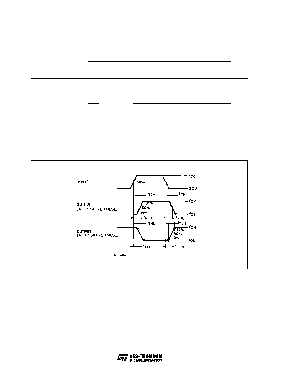
t
TLH
t
THL
Output Transition
Time
2.0
30
75
95
110
ns
4.5
8
15
19
22
6.0
7
13
16
19
t
PLH
t
PHL
Propagation
Delay Time
2.0
45
130
165
195
ns
4.5
15
26
33
39
6.0
13
22
28
33
C
IN
Input Capacitance
5
10
10
10
pF
C
PD
(*)
Power Dissipation
Capacitance
53
pF
(*) C
PD
is defined as the value of the IC's internal equivalent capacitance which is calculated from the operating current consumption without load.
(Refer to Test Circuit). Average operting current can be obtained by the following equation. I
CC
(opr) = C
PD
∑
V
CC
∑
f
IN
+ I
CC
SWITCHING CHARACTERISTICS TEST WAVEFORM
M54/M74HC155
5/11