1/8
September 2001
s
5V TOLERANT INPUTS
s
HIGH SPEED :
t
PD
= 5.2ns (MAX.) at V
CC
= 3V
s
POWER DOWN PROTECTION ON INPUTS
AND OUTPUTS
s
SYMMETRICAL OUTPUT IMPEDANCE:
|I
OH
| = I
OL
= 24mA (MIN) at V
CC
= 3V
s
PCI BUS LEVELS GUARANTEED AT 24 mA
s
OPERATING VOLTAGE RANGE:
V
CC
(OPR) = 2.0V to 3.6V (1.5V Data
Retention)
s
PIN AND FUNCTION COMPATIBLE WITH
74 SERIES 05
s
LATCH-UP PERFORMANCE EXCEEDS
500mA (JESD 17)
s
ESD PERFORMANCE:
HBM > 2000V (MIL STD 883 method 3015);
MM > 200V
DESCRIPTION
The 74LCX05 is a low voltage CMOS OPEN
DRAIN HEX INVERTER fabricated with
sub-micron silicon gate and double-layer metal
wiring C
2
MOS technology. It is ideal for low power
and high speed 3.3V applications. It can be
interfaced to 5V signal environment for inputs.
The internal circuit is composed of 3 stages
including buffer output, which provides high noise
immunity and stable output.
It has same speed performance at 3.3V than 5V
AC/ACT family, combined with a lower power
consumption.
All inputs and outputs are equipped with
protection circuits against static discharge, giving
them 2KV ESD immunity and transient excess
voltage.
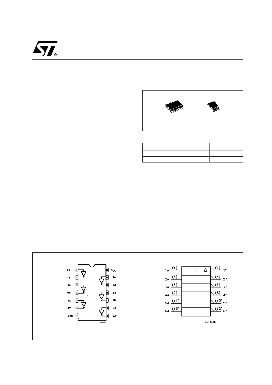
74LCX05
LOW VOLTAGE CMOS HEX INVERTER (OPEN DRAIN)
WITH 5V TOLERANT INPUTS
PIN CONNECTION AND IEC LOGIC SYMBOLS
ORDER CODES
PACKAGE
TUBE
T & R
SOP
74LCX05M
74LCX05MTR
TSSOP
74LCX05TTR
TSSOP
SOP
74LCX05
2/8
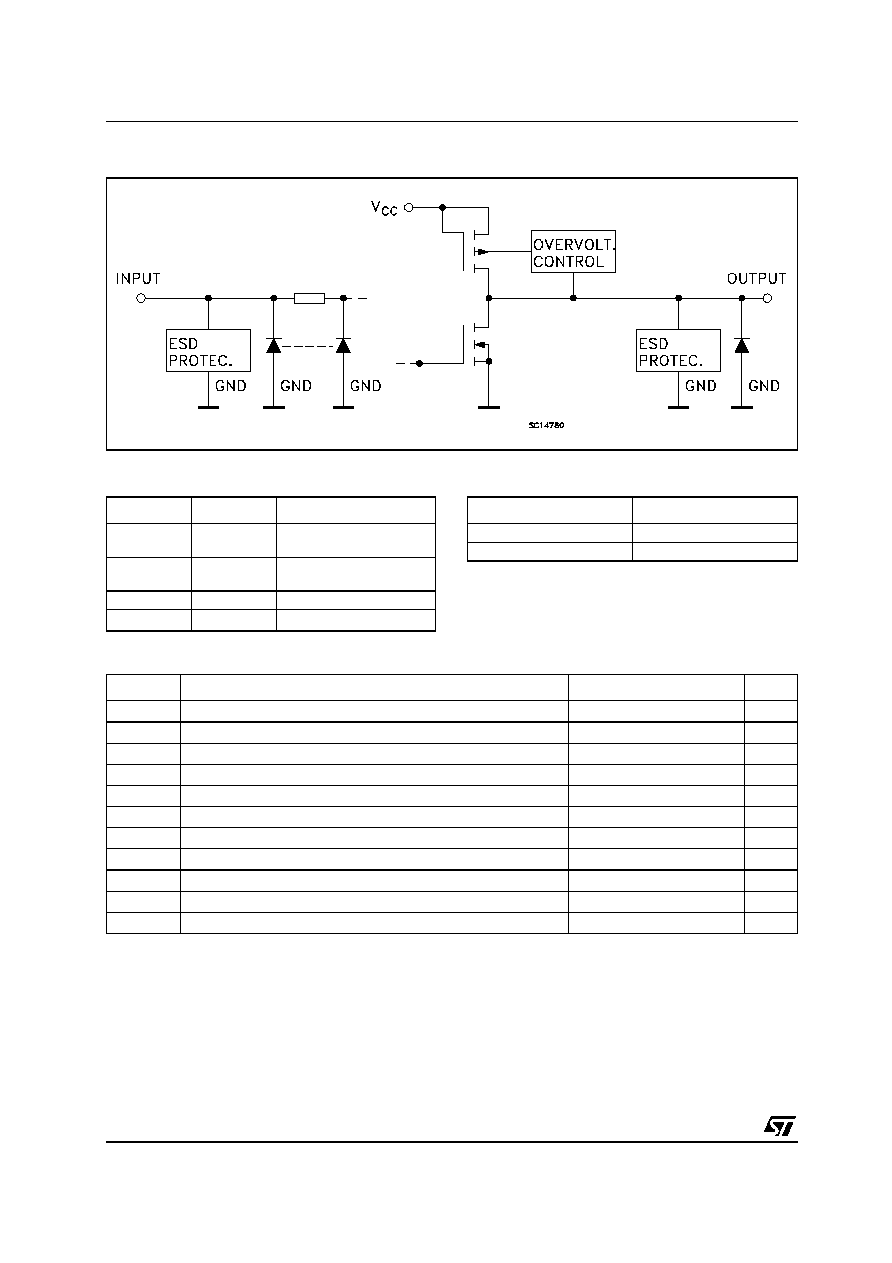
INPUT AND OUTPUT EQUIVALENT CIRCUIT
PIN DESCRIPTION
TRUTH TABLE
Z : High Impedance
ABSOLUTE MAXIMUM RATINGS
Absolute Maximum Ratings are those values beyond which damage to the device may occur. Functional operation under these conditions is
not implied
1) I
O
absolute maximum rating must be observed
2) V
O
< GND
PIN No
SYMBOL
NAME AND FUNCTION
1, 3, 5, 9, 11,
13
1A to 6A
Data Inputs
2, 4, 6, 8, 10,
12
1Y to 6Y
Data Outputs
7
GND
Ground (0V)
14
V
CC
Positive Supply Voltage
A
Y
L
Z
H
L
Symbol
Parameter
Value
Unit
V
CC
Supply Voltage
-0.5 to +7.0
V
V
I
DC Input Voltage
-0.5 to +7.0
V
V
O
DC Output Voltage (V
CC
= 0V)
-0.5 to +7.0
V
V
O
DC Output Voltage (High or Low State) (note 1)
-0.5 to V
CC
+ 0.5
V
I
IK
DC Input Diode Current
- 50
mA
I
OK
DC Output Diode Current (note 2)
- 50
mA
I
O
DC Output Current
�
50
mA
I
CC
DC Supply Current per Supply Pin
�
100
mA
I
GND
DC Ground Current per Supply Pin
�
100
mA
T
stg
Storage Temperature
-65 to +150
�C
T
L
Lead Temperature (10 sec)
300
�C
74LCX05
3/8
RECOMMENDED OPERATING CONDITIONS
1) Truth Table guaranteed: 1.5V to 3.6V
2) V
IN
from 0.8V to 2V at V
CC
= 3.0V
DC SPECIFICATIONS
DYNAMIC SWITCHING CHARACTERISTICS
1) Number of outputs defined as "n". Measured with "n-1" outputs switching from HIGH to LOW or LOW to HIGH. The remaining output is
measured in the LOW state.
Symbol
Parameter
Value
Unit
V
CC
Supply Voltage (note 1)
2.0 to 3.6
V
V
I
Input Voltage
0 to 5.5
V
V
O
Output Voltage (V
CC
= 0V)
0 to 5.5
V
V
O
Output Voltage (High or Low State)
0 to V
CC
V
I
OH
, I
OL
High or Low Level Output Current (V
CC
= 3.0 to 3.6V)
�
24
mA
I
OH
, I
OL
High or Low Level Output Current (V
CC
= 2.7V)
�
12
mA
T
op
Operating Temperature
-55 to 125
�C
dt/dv
Input Rise and Fall Time (note 2)
0 to 10
ns/V
Symbol
Parameter
Test Condition
Value
Unit
V
CC
(V)
-40 to 85 �C
-55 to 125 �C
Min.
Max.
Min.
Max.
V
IH
High Level Input
Voltage
2.7 to 3.6
2.0
2.0
V
V
IL
Low Level Input
Voltage
0.8
0.8
V
V
OL
Low Level Output
Voltage
2.7 to 3.6
I
O
=100
�
A
0.2
0.2
V
2.7
I
O
=12 mA
0.4
0.4
3.0
I
O
=16 mA
0.4
0.4
I
O
=24 mA
0.55
0.55
I
I
Input Leakage
Current
2.7 to 3.6
V
I
= 0 to 5.5V
�
5
�
5
�
A
I
off
Power Off Leakage
Current
0
V
I
or V
O
= 5.5V
10
10
�
A
I
OZ
High Impedance
Output Leakage
Current
2.7 to 3.6
V
I
= V
IH
or V
IL
V
O
= 0 to V
CC
�
5
�
5
�
A
I
CC
Quiescent Supply
Current
2.7 to 3.6
V
I
= V
CC
or GND
10
10
�
A
V
I
or V
O
= 3.6 to 5.5V
�
10
�
10
I
CC
I
CC
incr. per Input
2.7 to 3.6
V
IH
= V
CC
- 0.6V
500
500
�
A
Symbol
Parameter
Test Condition
Value
Unit
V
CC
(V)
T
A
= 25 �C
Min.
Typ.
Max.
V
OLP
Dynamic Low Level Quiet
Output (note 1)
3.3
V
IL
= 0V
V
IH
= 3.3V
0.8
V
V
OLV
-0.8
74LCX05
4/8
AC ELECTRICAL CHARACTERISTICS
1) Skew is defined as the absolute value of the difference between the actual propagation delay for any two outputs of the same device switch-
ing in the same direction, either HIGH or LOW (t
OSLH
= | t
PLHm
- t
PLHn
|, t
OSHL
= | t
PHLm
- t
PHLn
|)
2) Parameter guaranteed by design
CAPACITIVE CHARACTERISTICS
1) C
PD
is defined as the value of the IC's internal equivalent capacitance which is calculated from the operating current consumption without
load. (Refer to Test Circuit). Average operating current can be obtained by the following equation. I
CC(opr)
= C
PD
x V
CC
x f
IN
+ I
CC
/6 (per gate)
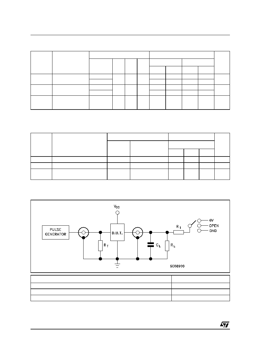
TEST CIRCUIT
C
L
= 50 pF or equivalent (includes jig and probe capacitance)
R
L
= R1 = 500
or equivalent
R
T
= Z
OUT
of pulse generator (typically 50
)
Symbol
Parameter
Test Condition
Value
Unit
V
CC
(V)
C
L
(pF)
R
L
(
)
t
s
= t
r
(ns)
-40 to 85 �C
-55 to 125 �C
Min.
Max.
Min.
Max.
t
PLZ
Propagation Delay
Time
2.7
50
500
2.5
6.5
6.5
ns
3.0 to 3.6
1.0
5.2
1.0
5.2
t
PZL
Propagation Delay
Time
2.7
50
500
2.5
6.5
6.5
ns
3.0 to 3.6
1.0
5.2
1.0
5.2
t
OSLH
t
OSHL
Output To Output
Skew Time (note1,
2)
3.0 to 3.6
50
500
2.5
1.0
1.0
ns
Symbol
Parameter
Test Condition
Value
Unit
V
CC
(V)
T
A
= 25 �C
Min.
Typ.
Max.
C
IN
Input Capacitance
3.3
V
IN
= 0 to V
CC
6
pF
C
OUT
Output Capacitance
3.3
V
IN
= 0 to V
CC
14
pF
C
PD
Power Dissipation Capacitance
(note 1)
3.3
f
IN
= 10MHz
V
IN
= 0 or V
CC
5
pF
TEST
SWITCH
t
PLH
, t
PHL
Open
t
PZL
, t
PLZ
6V
t
PZH
, t
PHZ
GND
74LCX05
5/8
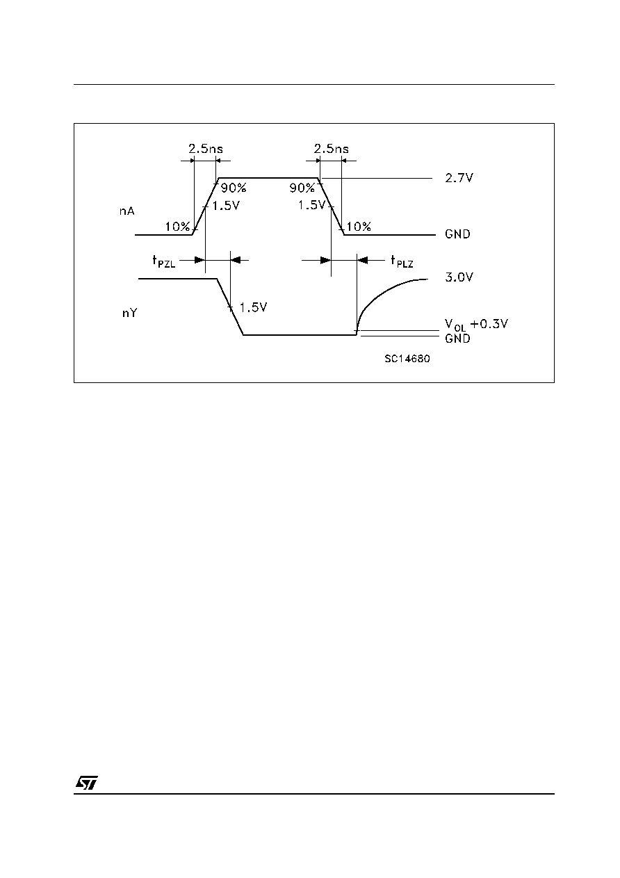
WAVEFORM : PROPAGATION DELAY (f=1MHz; 50% duty cycle)