1/9
February 2003
s
5V TOLERANT INPUTS AND OUTPUTS
s
HIGH SPEED:
t
PD
= 4.1 ns (MAX.) at V
CC
= 5V
s
LOW POWER DISSIPATION:
I
CC
= 2
µ
A (MAX.) at T
A
=25∞C
s
HIGH NOISE IMMUNITY:
V
NIH
= V
NIL
= 28% V
CC
(MIN.)
s
POWER DOWN PROTECTION ON INPUTS
AND OUPUTS
s
SYMMETRICAL OUTPUT IMPEDANCE:
|I
OH
| = I
OL
= 24 mA (MIN)
s
BALANCED PROPAGATION DELAYS:
t
PLH
t
PHL
s
OPERATING VOLTAGE RANGE:
V
CC
(OPR) = 2V to 3.6V (1.5V Data Retention)
s
PIN AND FUNCTION COMPATIBLE WITH
74 SERIES 16541
s
IMPROVED LATCH-UP IMMUNITY
s
ESD PERFORMANCE:
HBM>2000V(MIL STD 883 method 3015);
MM>200V
DESCRIPTION
The 74LCX16541 is an advanced high-speed
CMOS 16-BIT BUS BUFFER (3-STATE) fabricat-
ed with sub-micron silicon gate and double-layer
metal wiring C
2
MOS tecnology.
This is composed of two 8-bit sections with
separate output-enable signals. For either 8-bit
buffers section, the
3 STATE control gate
operates as a two input AND such that if either
nG1 and nG2 are high, all outputs are in the high
impedence state. This device is designed to be
used with 3 state memory address driveres, etc.
It hase same speed performance at 3.3V than 5V
AC/ACT family, combined with a lower power con-
sumption.
All inputs and outputs are equipped with protec-
tion circuits against static discharge, giving them
2KV ESD immunity and transient excess voltage.
74LCX16541
LOW VOLTAGE CMOS 16-BIT BUS BUFFER (3-STATE)
WITH 5V TOLERANT INPUTS/OUTPUTS (NON INVERTED)
ORDER CODES
PACKAGE
TUBE
T & R
TSSOP
74LCX16541TTR
TSSOP
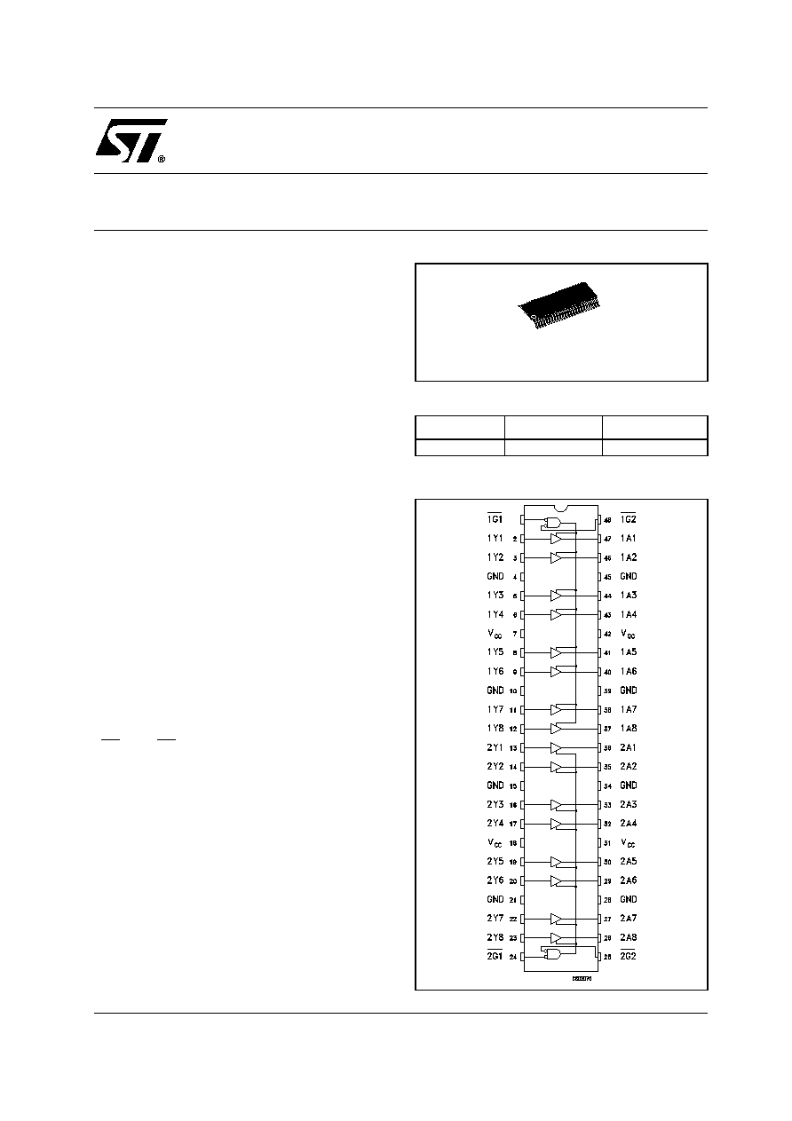
PIN CONNECTION

74LCX16541
2/9
INPUT AND OUTPUT EQUIVALENT CIRCUIT
PIN DESCRIPTION
TRUTH TABLE
X : Don't Care
Z : High Impedance
IEC LOGIC SYMBOLS
PIN No
SYMBOL
NAME AND FUNCTION
1, 48
1G1, 1G2
Output Enable Inputs
2, 3, 5, 6, 8, 9,
11, 12
1Y1 to 1Y8 Data Outputs
13, 14, 16, 17,
19, 20, 22, 23
2Y1 to 2Y8 Data Outputs
24, 25
2G1, 2G2
Output Enable Inputs
36, 35, 33, 32,
30, 29, 27, 26
2A1 to 2A8 Data Outputs
47, 46, 44, 43,
41, 40, 38, 37
1A1 to 1A8 Data Outputs
4, 10, 15, 21,
28, 34, 39, 45
GND
Ground (0V)
7, 18, 31, 42
V
CC
Positive Supply Voltage
INPUTS
OUTPUT
G1
G2
An
Yn
H
X
X
Z
X
H
X
Z
L
L
H
H
L
L
L
L

74LCX16541
3/9
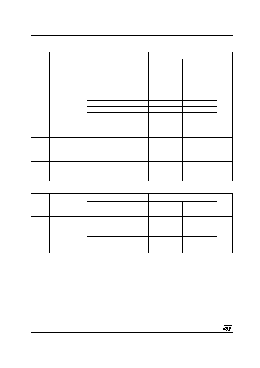
ABSOLUTE MAXIMUM RATINGS
Absolute Maximum Ratings are those values beyond which damage to the device may occur. Functional operation under these conditions is
not implied
1) Io absolute maximum rating must be observed
2)Vo < GND
RECOMMENDED OPERATING CONDITIONS
1) Truth Table guaranteed: 1.5V to 3.6V
2) V
IN
from0.8V to 2V at V
CC
=3.0V
Symbol
Parameter
Value
Unit
V
CC
Supply Voltage
-0.5 to +7.0
V
V
I
DC Input Voltage
-0.5 to +7.0
V
V
O
DC Output Voltage
-0.5 to +7.0
V
V
O
DC Output Voltage (High or Low State) (note 1)
-0.5 to Vcc+0.5
V
I
IK
DC Input Diode Current
-50
mA
I
OK
DC Output Diode Current (note 2)
-
50
mA
I
O
DC Output Current
+
50
mA
I
CC
or I
GND
DC V
CC
or Ground Current
±
100
mA
T
stg
Storage Temperature
-65 to +150
∞C
T
L
Lead Temperature (10 sec)
300
∞C
Symbol
Parameter
Value
Unit
V
CC
Supply Voltage (note 1)
2 to 3.6
V
V
I
Input Voltage
0 to 5.5
V
V
O
Output Voltage (OFF State)
0 to 5.5
V
V
O
Output Voltage (High or Low State)
0 to Vcc
V
T
op
Operating Temperature
-55 to 125
∞C
I
OH,
I
OL
High or Low Level Output Current (Vcc = 3.0 to 3.6V)
±
24
mA
I
OH,
I
OL
High or Low Level Output Current (Vcc = 2.7V)
±
12
mA
dt/dv
Input Rise and Fall Time (note 2)
0 to 10
ns/V
74LCX16541
4/9
DC SPECIFICATIONS
AC ELECTRICAL CHARACTERISTICS ( C
L
= 50 pF, R
L
= 500
, Input t
r
= t
f
= 2.5ns)
Symbol
Parameter
Test Condition
Value
Unit
V
CC
(V)
-40 to 85 ∞C
-55 to 125 ∞C
Min.
Max.
Min.
Max.
V
IH
High Level Input
Voltage
2.7 to 3.6
2.0
2.0
V
V
IL
Low Level Input
Voltage
0.8
0.8
V
V
OH
High Level Output
Voltage
2.7 to 3.6
I
O
=-100
µ
A
V
CC
-0.2
V
CC
-0.2
V
2.7
I
O
=-12 mA
2.2
2.2
3.0
I
O
=-12 mA
2.4
2.4
3.0
I
O
=-24 mA
2.2
2.2
V
OL
Low Level Output
Voltage
2.7 to 3.6
I
O
=100
µ
A
0.2
0.2
V
2.7
I
O
=12 mA
0.4
0.4
3.0
I
O
=24 mA
0.55
0.55
I
OZ
High Impedance
Output Leakage
Current
2.7 to 3.6
V
I
= 0 to 5.5V
±
5
±
5
µ
A
I
I
Input Leakage
Current
2.7 to 3.6
V
I
= 0 to 5.5V
±
5
±
5
µ
A
I
off
Power Off Leakage
Current
0
V
I
or V
O
= 5.5V
10
10
µ
A
I
CC
Quiescent Supply
Current
2.7 to 3.6
V
I
= V
CC
or GND
20
20
µ
A
Symbol
Parameter
Test Condition
Value
Unit
V
CC
(V)
C
L
(pF)
-40 to 85∞C
-55 to 125∞C
Min.
Max.
Min.
Max.
t
PLH
t
PHL
Propagation Delay
Time
A to Y
2.7
1.5
4.7
1.5
4.7
ns
3.0 to 3.6
1.5
4.1
1.5
4.1
t
PZL
t
PZH
Output Enable Time
2.7
1.5
5.8
1.5
5.8
ns
3.0 to 3.6
1.5
4.6
1.5
4.6
t
PLZ
t
PHZ
Output Disable Time
2.7
1.5
6.2
1.5
6.2
ns
3.0 to 3.6
1.5
5.8
1.5
5.8
74LCX16541
5/9
CAPACITIVE CHARACTERISTICS
1) C
PD
is defined as the value of the IC's internal equivalent capacitance which is calculated from the operating current consumption without
load. (Refer to Test Circuit). Average operating current can be obtained by the following equation. I
CC(opr)
= C
PD
x V
CC
x f
IN
+ I
CC
/ 16
TEST CIRCUIT
C
L
= 50 pF or equivalent (includes jig and probe capacitance)
R
L
= R1 = 500
or equivalent
R
T
= Z
OUT
of pulse generator (typically 50
)
Symbol
Parameter
Test Condition
Value
Unit
V
CC
(V)
T
A
= 25 ∞C
Min.
Typ.
Max.
C
IN
Input Capacitance
3.3
V
I
= 0V or V
CC
4
pF
C
OUT
Output Capacitance
3.3
V
I
= 0V or V
CC
10
pF
C
PD
Power Dissipation Capacitance
(note 1) Output enabled
2.5
f
IN
= 10MHz
V
I
= 0V or V
CC
45
pF
3.3
50
Power Dissipation Capacitance
(note 1) Output disabled
2.5
f
IN
= 10MHz
V
I
= 0V or V
CC
3
pF
3.3
4
TEST
SWITCH
t
PLH
, t
PHL
Open
t
PZL
, t
PLZ
2V
CC
t
PZH
, t
PHZ
GND
74LCX16541
6/9
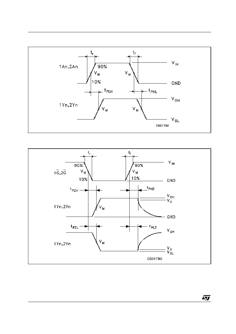
WAVEFORM 1: PROPAGATION DELAYS (f=1MHz; 50% duty cycle)
WAVEFORM 2: OUTPUT ENABLE AND DISABLE TIME (f=1MHz; 50% duty cycle; V
Y
= V
OH
-03V,
V
X
= V
OL
+0.3V)
74LCX16541
7/9
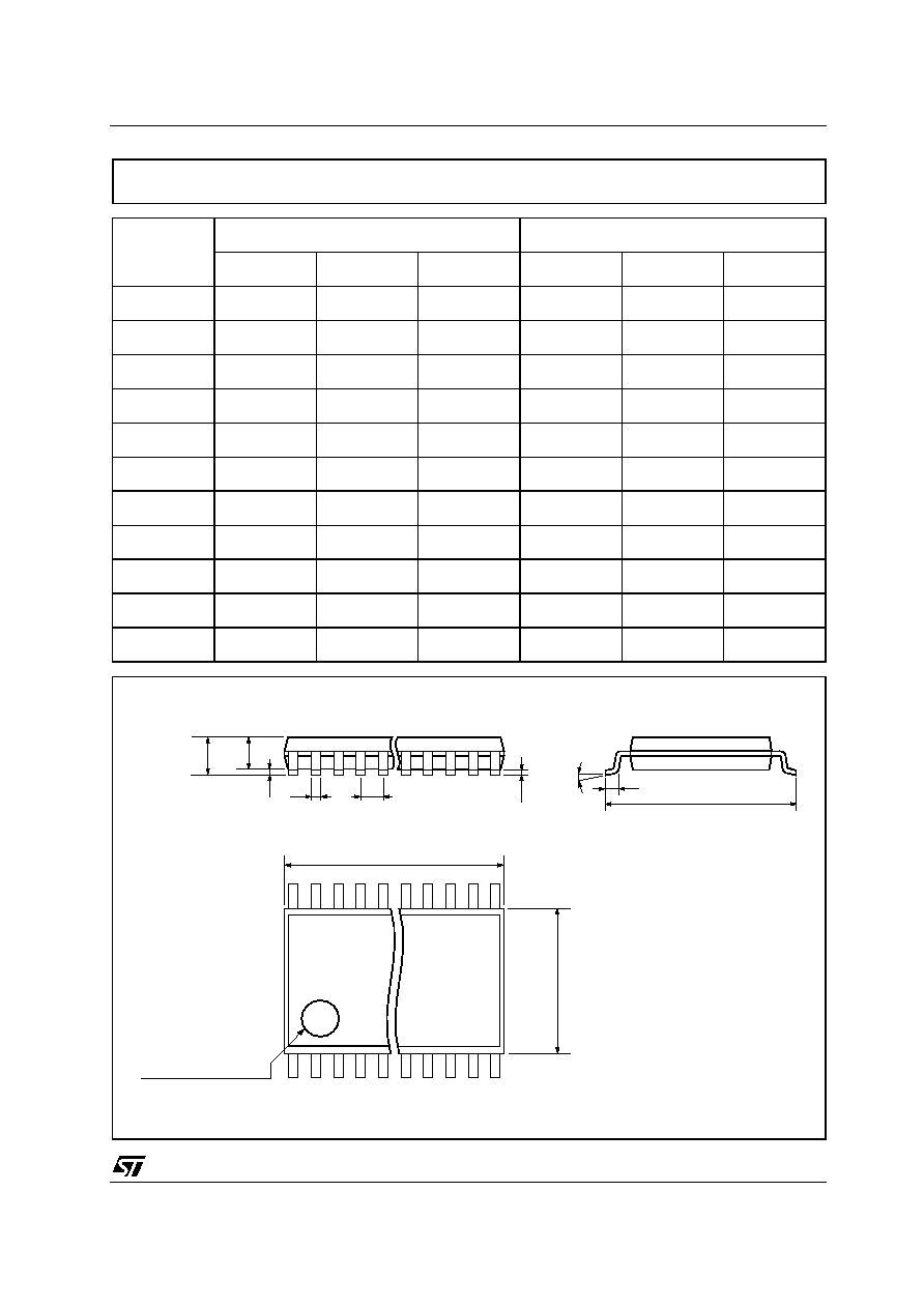
DIM.
mm.
inch
MIN.
TYP
MAX.
MIN.
TYP.
MAX.
A
1.2
0.047
A1
0.05
0.15
0.002
0.006
A2
0.9
0.035
b
0.17
0.27
0.0067
0.011
c
0.09
0.20
0.0035
0.0079
D
12.4
12.6
0.488
0.496
E
8.1 BSC
0.318 BSC
E1
6.0
6.2
0.236
0.244
e
0.5 BSC
0.0197 BSC
K
0∞
8∞
0∞
8∞
L
0.50
0.75
0.020
0.030
TSSOP48 MECHANICAL DATA
c
E
b
A2
A
E1
D
1
PIN 1 IDENTIFICATION
A1
L
K
e
7065588C
74LCX16541
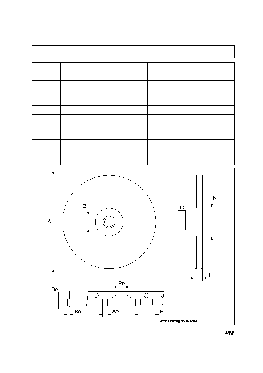
8/9
DIM.
mm.
inch
MIN.
TYP
MAX.
MIN.
TYP.
MAX.
A
330
12.992
C
12.8
13.2
0.504
0.519
D
20.2
0.795
N
60
2.362
T
30.4
1.197
Ao
8.7
8.9
0.343
0.350
Bo
13.1
13.3
0.516
0.524
Ko
1.5
1.7
0.059
0.067
Po
3.9
4.1
0.153
0.161
P
11.9
12.1
0.468
0.476
Tape & Reel TSSOP48 MECHANICAL DATA

74LCX16541
9/9
Information furnished is believed to be accurate and reliable. However, STMicroelectronics assumes no responsibility for the
consequences of use of such information nor for any infringement of patents or other rights of third parties which may result from
its use. No license is granted by implication or otherwise under any patent or patent rights of STMicroelectronics. Specifications
mentioned in this publication are subject to change without notice. This publication supersedes and replaces all information
previously supplied. STMicroelectronics products are not authorized for use as critical components in life support devices or
systems without express written approval of STMicroelectronics.
© The ST logo is a registered trademark of STMicroelectronics
© 2003 STMicroelectronics - Printed in Italy - All Rights Reserved
STMicroelectronics GROUP OF COMPANIES
Australia - Brazil - Canada - China - Finland - France - Germany - Hong Kong - India - Israel - Italy - Japan - Malaysia - Malta - Morocco
Singapore - Spain - Sweden - Switzerland - United Kingdom - United States.
© http://www.st.com