 | –≠–ª–µ–∫—Ç—Ä–æ–Ω–Ω—ã–π –∫–æ–º–ø–æ–Ω–µ–Ω—Ç: 74LCX244M | –°–∫–∞—á–∞—Ç—å:  PDF PDF  ZIP ZIP |

1/9
March 2002
s
5V TOLERANT INPUTS AND OUTPUTS
s
HIGH SPEED :
t
PD
= 6.5 ns (MAX.) at V
CC
= 3V
s
POWER DOWN PROTECTION ON INPUTS
AND OUTPUTS
s
SYMMETRICAL OUTPUT IMPEDANCE:
|I
OH
| = I
OL
= 24mA (MIN) at V
CC
= 3V
s
PCI BUS LEVELS GUARANTEED AT 24 mA
s
BALANCED PROPAGATION DELAYS:
t
PLH
t
PHL
s
OPERATING VOLTAGE RANGE:
V
CC
(OPR) = 2.0V to 3.6V (1.5V Data
Retention)
s
PIN AND FUNCTION COMPATIBLE WITH
74 SERIES 244
s
LATCH-UP PERFORMANCE EXCEEDS
500mA (JESD 17)
s
ESD PERFORMANCE:
HBM > 2000V (MIL STD 883 method 3015);
MM > 200V
DESCRIPTION
The 74LCX244 is a low voltage CMOS OCTAL
BUS BUFFER (NON-INVERTED) fabricated with
sub-micron silicon gate and double-layer metal
wiring C
2
MOS technology. It is ideal for low power
and high speed 3.3V applications; it can be
interfaced to 5V signal environment for both inputs
and outputs.
It has same speed performance at 3.3V than 5V
AC/ACT family, combined with a lower power
consumption.
This device is designed to be used with 3 state
memory address drivers, etc.
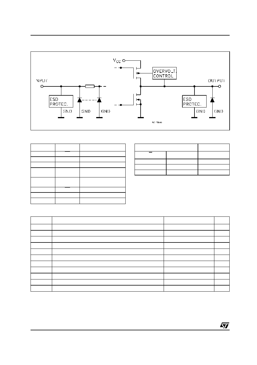
All
inputs
and
outputs
are
equipped
with
protection circuits against static discharge, giving
them 2KV ESD immunity and transient excess
voltage.
74LCX244
LOW VOLTAGE CMOS OCTAL BUS BUFFER (3-STATE)
WITH 5V TOLERANT INPUTS AND OUTPUTS
PIN CONNECTION AND IEC LOGIC SYMBOLS
ORDER CODES
PACKAGE
TUBE
T & R
SOP
74LCX244M
74LCX244MTR
TSSOP
74LCX244TTR
TSSOP
SOP
74LCX244
2/9
INPUT AND OUTPUT EQUIVALENT CIRCUIT
PIN DESCRIPTION
TRUTH TABLE
X : Don't Care
Z : High Impedance
ABSOLUTE MAXIMUM RATINGS
Absolute Maximum Ratings are those values beyond which damage to the device may occur. Functional operation under these conditions is
not implied
1) I
O
absolute maximum rating must be observed
2) V
O
< GND
PIN No
SYMBOL
NAME AND FUNCTION
1
1G
Output Enable Input
2, 4, 6, 8
1A1 to 1A4
Data Inputs
9, 7, 5, 3
2Y1 to 2Y4
Data Outputs
11, 13, 15,
17
2A1 to 2A4
Data Inputs
18, 16, 14,
12
1Y1 to 1Y4
Data Outputs
19
2G
Output Enable Input
10
GND
Ground (0V)
20
V
CC
Positive Supply Voltage
INPUT
OUTPUT
G
An
Yn
L
L
L
L
H
H
H
X
Z
Symbol
Parameter
Value
Unit
V
CC
Supply Voltage
-0.5 to +7.0
V
V
I
DC Input Voltage
-0.5 to +7.0
V
V
O
DC Output Voltage (OFF State)
-0.5 to +7.0
V
V
O
DC Output Voltage (High or Low State) (note 1)
-0.5 to V
CC
+ 0.5
V
I
IK
DC Input Diode Current
- 50
mA
I
OK
DC Output Diode Current (note 2)
- 50
mA
I
O
DC Output Current
±
50
mA
I
CC
DC Supply Current per Supply Pin
±
100
mA
I
GND
DC Ground Current per Supply Pin
±
100
mA
T
stg
Storage Temperature
-65 to +150
∞
C
T
L
Lead Temperature (10 sec)
300
∞
C

74LCX244
3/9
RECOMMENDED OPERATING CONDITIONS
1) Truth Table guaranteed: 1.5V to 3.6V
2) V
IN
from 0.8V to 2V at V
CC
= 3.0V
DC SPECIFICATIONS
Symbol
Parameter
Value
Unit
V
CC
Supply Voltage (note 1)
2.0 to 3.6
V
V
I
Input Voltage
0 to 5.5
V
V
O
Output Voltage (OFF State)
0 to 5.5
V
V
O
Output Voltage (High or Low State)
0 to V
CC
V
I
OH
, I
OL
High or Low Level Output Current (V
CC
= 3.0 to 3.6V)
±
24
mA
I
OH
, I
OL
High or Low Level Output Current (V
CC
= 2.7V)
±
12
mA
T
op
Operating Temperature
-55 to 125
∞
C
dt/dv
Input Rise and Fall Time (note 2)
0 to 10
ns/V
Symbol
Parameter
Test Condition
Value
Unit
V
CC
(V)
-40 to 85
∞
C
-55 to 125
∞
C
Min.
Max.
Min.
Max.
V
IH
High Level Input
Voltage
2.7 to 3.6
2.0
2.0
V
V
IL
Low Level Input
Voltage
0.8
0.8
V
V
OH
High Level Output
Voltage
2.7 to 3.6
I
O
=-100
µ
A
V
CC
-0.2
V
CC
-0.2
V
2.7
I
O
=-12 mA
2.2
2.2
3.0
I
O
=-18 mA
2.4
2.4
I
O
=-24 mA
2.2
2.2
V
OL
Low Level Output
Voltage
2.7 to 3.6
I
O
=100
µ
A
0.2
0.2
V
2.7
I
O
=12 mA
0.4
0.4
3.0
I
O
=16 mA
0.4
0.4
I
O
=24 mA
0.55
0.55
I
I
Input Leakage
Current
2.7 to 3.6
V
I
= 0 to 5.5V
±
5
±
5
µ
A
I
off
Power Off Leakage
Current
0
V
I
or V
O
= 5.5V
10
10
µ
A
I
OZ
High Impedance
Output Leakage
Current
2.7 to 3.6
V
I
= V
IH
or V
IL
V
O
= 0 to V
CC
±
5
±
5
µ
A
I
CC
Quiescent Supply
Current
2.7 to 3.6
V
I
= V
CC
or GND
10
10
µ
A
V
I
or V
O
= 3.6 to 5.5V
±
10
±
10
I
CC
I
CC
incr. per Input
2.7 to 3.6
V
IH
= V
CC
- 0.6V
500
500
µ
A
74LCX244
4/9
DYNAMIC SWITCHING CHARACTERISTICS
1) Number of outputs defined as "n". Measured with "n-1" outputs switching from HIGH to LOW or LOW to HIGH. The remaining output is
measured in the LOW state.
AC ELECTRICAL CHARACTERISTICS
1) Skew is defined as the absolute value of the difference between the actual propagation delay for any two outputs of the same device switch-
ing in the same direction, either HIGH or LOW (t
OSLH
= | t
PLHm
- t
PLHn
|, t
OSHL
= | t
PHLm
- t
PHLn
|)
2) Parameter guaranteed by design
CAPACITIVE CHARACTERISTICS
1) C
PD
is defined as the value of the IC's internal equivalent capacitance which is calculated from the operating current consumption without
load. (Refer to Test Circuit). Average operating current can be obtained by the following equation. I
CC(opr)
= C
PD
x V
CC
x f
IN
+ I
CC
/8 (per circuit)
Symbol
Parameter
Test Condition
Value
Unit
V
CC
(V)
T
A
= 25
∞
C
Min.
Typ.
Max.
V
OLP
Dynamic Low Level Quiet
Output (note 1)
3.3
C
L
= 50pF
V
IL
= 0V, V
IH
= 3.3V
0.8
V
V
OLV
-0.8
Symbol
Parameter
Test Conditi on
Value
Unit
V
CC
(V)
C
L
(pF)
R
L
(
)
t
s
= t
r
(ns)
-40 to 85
∞
C
-55 to 125
∞
C
Min.
Max.
Min.
Max.
t
PLH
t
PHL
Propagation Delay
Time
2.7
50
500
2.5
1.5
7.5
1.5
8.2
ns
3.0 to 3.6
1.5
6.5
1.5
7.1
t
PZL
t
PZH
Output Enable Time
2.7
50
500
2.5
1.5
9.0
1.5
10.5
ns
3.0 to 3.6
1.5
8.0
1.5
9.2
t
PLZ
t
PHZ
Output Disable Time
2.7
50
500
2.5
1.5
8.0
1.5
9.2
ns
3.0 to 3.6
1.5
7.0
1.5
7.7
t
OSLH
t
OSHL
Output To Output
Skew Time (note1,
2)
3.0 to 3.6
50
500
2.5
1.0
1.0
ns
Symbol
Parameter
Test Condition
Value
Unit
V
CC
(V)
T
A
= 25
∞
C
Min.
Typ.
Max.
C
IN
Input Capacitance
3.3
V
IN
= 0 to V
CC
6
pF
C
OUT
Output Capacitance
3.3
V
IN
= 0 to V
CC
10
pF
C
PD
Power Dissipation Capacitance
(note 1)
3.3
f
IN
= 10MHz
V
IN
= 0 or V
CC
34
pF
74LCX244
5/9
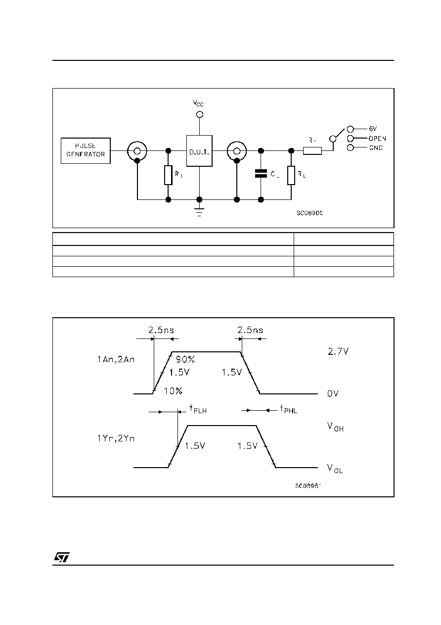
TEST CIRCUIT
C
L
= 50 pF or equivalent (includes jig and probe capacitance)
R
L
= R1 = 500
or equivalent
R
T
= Z
OUT
of pulse generator (typically 50
)
WAVEFORM 1 : PROPAGATION DELAYS (f=1MHz; 50% duty cycle)
TEST
SWIT CH
t
PLH
, t
PHL
Open
t
PZL
, t
PLZ
6V
t
PZH
, t
PHZ
GND

74LCX244
6/9
WAVEFORM 2 : OUTPUT ENABLE AND DISABLE TIME (f=1MHz; 50% duty cycle)
74LCX244
7/9
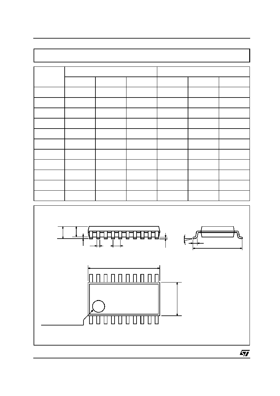
DIM.
mm.
inch
MIN.
TYP
MAX.
MIN.
TYP.
MAX.
A
2.65
0.104
a1
0.1
0.2
0.004
0.008
a2
2.45
0.096
b
0.35
0.49
0.014
0.019
b1
0.23
0.32
0.009
0.012
C
0.5
0.020
c1
45
∞
(typ.)
D
12.60
13.00
0.496
0.512
E
10.00
10.65
0.393
0.419
e
1.27
0.050
e3
11.43
0.450
F
7.40
7.60
0.291
0.300
L
0.50
1.27
0.020
0.050
M
0.75
0.029
S
8
∞
(max.)
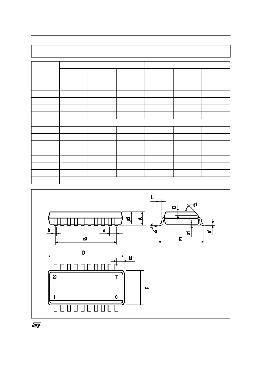
SO-20 MECHANICAL DATA
PO13L
74LCX244
8/9
DIM.
mm.
inch
MIN.
TYP
MAX.
MIN.
TYP.
MAX.
A
1.2
0.047
A1
0.05
0.15
0.002
0.004
0.006
A2
0.8
1
1.05
0.031
0.039
0.041
b
0.19
0.30
0.007
0.012
c
0.09
0.20
0.004
0.0089
D
6.4
6.5
6.6
0.252
0.256
0.260
E
6.2
6.4
6.6
0.244
0.252
0.260
E1
4.3
4.4
4.48
0.169
0.173
0.176
e
0.65 BSC
0.0256 BSC
K
0
∞
8
∞
0
∞
8
∞
L
0.45
0.60
0.75
0.018
0.024
0.030
TSSOP20 MECHANICAL DATA
c
E
b
A2
A
E1
D
1
PIN 1 IDENTIFICATION
A1
L
K
e
0087225C

74LCX244
Information furnished is believed to be accurate and reliable. However, STMicroelectronics assumes no responsibility for the
consequences of use of such inform ation nor for any infringe ment of patents or other righ ts of third parties which may result from
its use. No license is granted by implication or otherwise under any patent or patent rights of STMicroelectronics. Specifications
mentioned in this pub lication are subject to change without notice. Thi s pub lication supersedes and replaces all information
previously supplied. STMicroelectronics prod ucts are not authori zed for use as critical components in life suppo rt devices or
systems without express written approval of STMicroelectronics.
©
The ST logo is a registered trademark of STMicroelectronics
©
2000 STMicroelectronics - Printed in Italy - All Rights Reserved
STMicroelectronics GROUP OF COMPANIES
Australia - Brazil - China - Finland - France - Germany - Hong Kong - India - Italy - Japan - Malaysia - Malta - Morocco
Singapore - Spain - Sweden - Swit zerland - United Kingdom
©
http://w ww.st.com
9/9