 | –≠–ª–µ–∫—Ç—Ä–æ–Ω–Ω—ã–π –∫–æ–º–ø–æ–Ω–µ–Ω—Ç: 74LCX374 | –°–∫–∞—á–∞—Ç—å:  PDF PDF  ZIP ZIP |
74LCX374
OCTAL D-TYPE FLIP FLOP NON INVERTING (3-STATE)
WITH 5V TOLERANT INPUTS AND OUTPUTS
Æ
February 1999
s
5V TOLERANT INPUTS AND OUTPUTS
s
HIGH SPEED:
f
MAX
= 150 MHz (MIN.) at V
CC
= 3V
s
POWER-DOWN PROTECTION ON INPUTS
AND OUTPUTS
s
SYMMETRICAL OUTPUT IMPEDANCE:
|I
OH
| = I
OL
= 24 mA (MIN)
s
PCI BUS LEVELS GUARANTEED AT 24mA
s
BALANCED PROPAGATION DELAYS:
t
PLH
t
PHL
s
OPERATING VOLTAGE RANGE:
V
CC
(OPR) = 2.0V to 3.6V (1.5V Data Retention)
s
PIN AND FUNCTION COMPATIBLE WITH
74 SERIES 374
s
LATCH-UP PERFORMANCE EXCEEDS 500mA
s
ESD PERFORMANCE:
HBM >2000V; MM > 200V
DESCRIPTION
The LCX374 is a low voltage CMOS OCTAL
D-TYPE FLIP FLOP with 3 STATE OUTPUT
NON INVERTING fabricated with sub-micron
silicon gate and double-layer metal wiring C
2
MOS
technology. It is ideal for low power and high
speed applications; it can be interfaced to 5V
signal environment for both inputs and outputs.
These 8 bit D-Type flip-flops are controlled by a
clock input (CK) and an output enable input (OE).
On the positive transition of the clock, the Q
outputs will be set to the logic state that were
setup at the D inputs.
While the (OE) input is low, the 8 outputs will be
in a normal state (high or low logic level) and
while high level the outputs will be in a high
impedance state.
The output control does not affect the internal
operation of flip flops; that is, the old data can be
retained or the new data can be entered even
while the outputs are off.
It has same speed performance at 3.3V than 5V,
AC/ACT family, combined with a lower power
consumption. It has better speed performance at
3.3V than 5V LSTTL family combined with the
true CMOS low power consumption.
All inputs
and
outputs are
equipped with
protection circuits against static discharge, giving
them 2KV ESD immunity and transient excess
voltage.
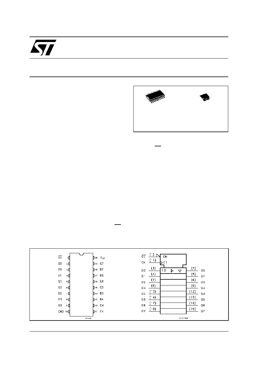
PIN CONNECTION AND IEC LOGIC SYMBOLS
ORDER CODES :
74LCX374M
74LCX374T
M
(Micro Package)
T
(TSSOP Package)
1/10
PIN DESCRIPTION
PI N No
SYMBOL
NAME AND FUNCT ION
1
OE
3 State Output Enable
Input (Active LOW)
2, 5, 6, 9,
12, 15, 16,
19
Q0 to Q7
3 State Outputs
3, 4, 7, 8,
13, 14, 17,
18
D0 to D7
Data Inputs
11
CLOCK
Clock Input (LOW to
HIGH, edge triggered)
10
GND
Ground (0V)
20
V
CC
Positive Supply Voltage
TRUTH TABLE
INPUT S
OUT PUT S
OE
CK
D
Q
H
X
X
Z
L
X
NO CHANGE
L
L
L
L
H
H
X:"H" or "L"
Z: High Impedance
LOGIC DIAGRAM
INPUT AND OUTPUT EQUIVALENT CIRCUIT
74LCX374
2/10

RECOMMENDED OPERATING CONDITIONS
Symbol
Parameter
Value
Unit
V
CC
Supply Voltage (note 1)
2.0 to 3.6
V
V
I
Input Voltage
0 to 5.5
V
V
O
Output Voltage (OFF state)
0 to 5.5
V
V
O
Output Voltage (High or Low State)
0 to V
CC
V
I
OH
, I
OL
High or Low Level Output Current (V
CC
= 3.0 to 3.6V)
±
24
mA
I
OH
, I
OL
High or Low Level Output Current (V
CC
= 2.7 to 3.0V)
±
12
mA
T
op
Operating Temperature:
-40 to +85
o
C
dt/dv
Input Transition Rise or Fall Rate (V
CC
= 3.0V) (note 2)
0 to 10
ns/V
1) Truth Table guaranteed: 1.5V to3.6V
2) V
IN
from0.8V to 2.0V
ABSOLUTE MAXIMUM RATINGS
Symbol
Parameter
Val ue
Unit
V
CC
Supply Voltage
-0.5 to + 7.0
V
V
I
DC Input Voltage
-0.5 to + 7.0
V
V
O
DC Output Voltage (OFF state)
-0.5 to + 7.0
V
V
O
DC Output Voltage (High or Low State) (note1)
-0.5 to V
CC
+ 0.5
V
I
IK
DC Input Diode Current
- 50
mA
I
OK
DC Output Diode Current (note2)
±
50
mA
I
O
DC Output Source/Sink Current
±
50
mA
I
CC
DC Supply Current per Supply Pin
±
100
mA
I
GND
DC Ground Current per Supply Pin
±
100
mA
T
stg
Storage Temperature
-65 to +150
o
C
T
L
Lead Temperature (10 sec)
300
o
C
Absolute Maximum Ratings are those values beyond which damage to the device may occur. Functional operation under these condition is not implied.
1) I
O
absolute maximum rating must be observed
2) V
O
< GND, V
O
> V
CC
74LCX374
3/10
DC SPECIFICATIONS
Symb ol
Parameter
Test Co ndi ti ons
Value
Un it
V
CC
(V)
-40 to 85
o
C
Min.
Max.
V
IH
High Level Input Voltage
2. 7 t o 3.6
2.0
V
V
IL
Low Level Input Voltage
0.8
V
V
OH
High Level Output Voltage
2.7 to 3.6
V
I
=
V
I H
or
V
IL
I
O
=-100
µ
A
V
CC
-0.2
V
2.7
I
O
=-12 mA
2.2
3.0
I
O
=-18 mA
2.4
I
O
=-24 mA
2.2
V
OL
Low Level Output Voltage
2.7 to 3.6
V
I
=
V
I H
or
V
IL
I
O
=100
µ
A
0.2
V
2.7
I
O
=12 mA
0.4
3.0
I
O
=16 mA
0.4
3.0
I
O
=24 mA
0.55
I
I
Input Leakage Current
2. 7 t o 3.6
V
I
= 0 to 5.5 V
±
5
µ
A
I
OZ
3 State Output Leakage Current
2.7 to 3.6
V
I
= V
IH
or V
IL
V
O
= 0 to 5.5V
±
5
µ
A
I
off
Power Off Leakage Current
0
V
I
or V
O
= 5.5V
100
µ
A
I
CC
Quiescent Supply Current
2.7 to 3.6
V
I
= V
CC
or GND
10
µ
A
V
I
or V
O
=
3.6 to 5.5V
±
10
I
CC
ICC incr. per input
2.7 to 3.6
V
IH
= V
CC
-0.6V
500
µ
A
DYNAMIC SWITCHING CHARACTERISTICS
Symb ol
Parameter
Test Con dition s
Value
Un it
V
CC
(V)
T
A
= 25
o
C
Min .
T yp.
Max.
V
OLP
Dynamic Low Voltage Quiet Output
(note 1)
3.3
C
L
= 50 pF
V
IL
= 0 V
V
IH
= 3. 3V
0.8
V
V
OLV
-0.8
1) Number ofoutputs defined as "n". Measured with"n-1" outputs switching from HIGH to LOW or LOW t o HIGH. The remaining output is measured in
the LOW state.
74LCX374
4/10

CAPACITIVE CHARACTERISTICS
Symb ol
Parameter
Test Co ndi ti ons
Valu e
Un it
V
CC
(V)
T
A
= 25
o
C
Mi n.
T yp.
Max.
C
IN
Input Capacitance
3.3
V
IN
= 0 to V
CC
6
pF
C
OUT
Output Capacitance
3.3
V
IN
= 0 to V
CC
12
pF
C
PD
Power Dissipation Capacitance (note 1)
3.3
f
IN
= 10MHz
V
IN
= 0 or V
CC
32
pF
1) C
PD
isdefined as the value of the IC'sinternal equivalent capacitance which is calculated fromthe operating current consumption without load. Average
operting current can be obtained by the following equation. I
CC
(opr) = C
PD
∑
V
CC
∑
f
IN
+ I
CC
/8 (per Flip-Flop)
AC ELECTRICAL CHARACTERISTICS (C
L
= 50 pF, R
L
= 500
, Input t
r
= t
f
= 2.5 ns)
Symb ol
Parameter
Test Con dition
Val ue
Un it
V
CC
(V)
Waveform
-40 to 85
o
C
Mi n.
Max.
t
PLH
t
PHL
Propagation Delay Time
2.7
1
1.5
9.5
ns
3.0 to 3.6
1.5
8.5
t
PZL
t
PZH
Output Enable Time to HIGH and LOW
level
2.7
2
1.5
9.5
ns
3.0 to 3.6
1.5
8.5
t
PLZ
t
PHZ
Output Disable Time from HIGh and
LOW level
2.7
2
1.5
8.5
ns
3.0 to 3.6
1.5
7.5
t
s
Setup Time, HIGh or LOW level Dn to
CK
2.7
1
2.5
ns
3.0 to 3.6
2.5
t
h
Hold Time, HIGh or LOW level Dn to CK
2.7
1
1.5
ns
3.0 to 3.6
1.5
t
w
CK Pulse Width, HIGH or LOW
2.7
3
3.3
ns
3.0 to 3.6
3.3
f
MAX
Clock Pulse Frequency
3.0 to 3.6
1
150
MHz
t
OSLH
t
OSHL
Output to Output Skew Time (note 1, 2)
3.0 to 3.6
1.0
ns
1) Skew is defined as the absolute value of the difference between the actual propagation delay for any twooutputs of the same device switching in the
same direction, either HIGH or LOW (t
OSLH
= |t
PLHm
- t
PLHn
|, t
OSHL
= |t
PHLm
- t
pHLn
|)
2) Parameter guaranteed by design
74LCX374
5/10
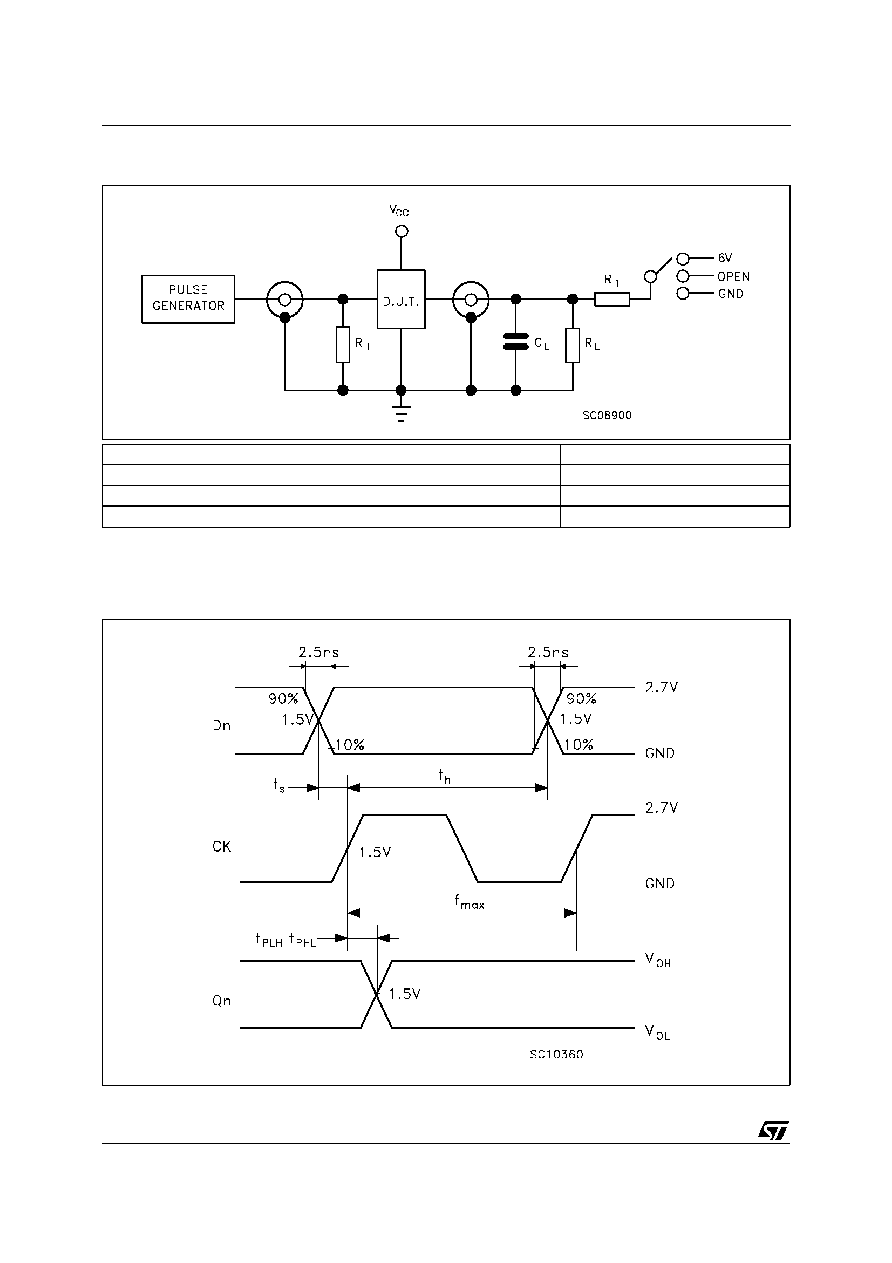
TEST CIRCUIT
T EST
SW IT CH
t
PLH
, t
PHL
Open
t
PZL
, t
PLZ
6V
t
PZH
, t
PHZ
GND
C
L
= 50 pF or equivalent (includes jigand probe capacitance)
R
L
= R
1
= 500
orequivalent
R
T
= Z
OUT
of pulse generator (typically 50
)
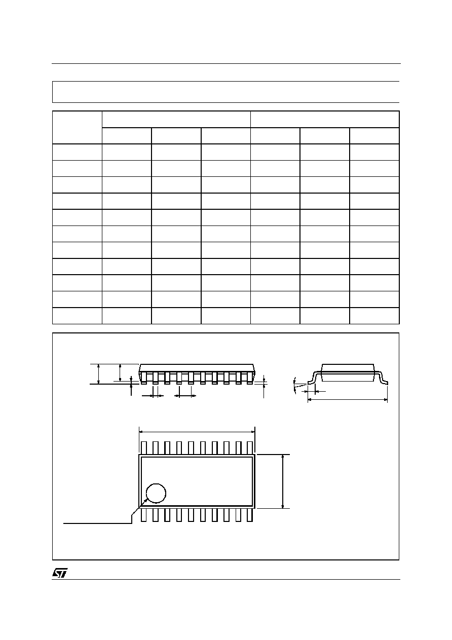
WAVEFORM 1: PROPAGATION DELAYS, SETUP AND HOLD TIMES (f=1MHz; 50% duty cicle)
74LCX374
6/10
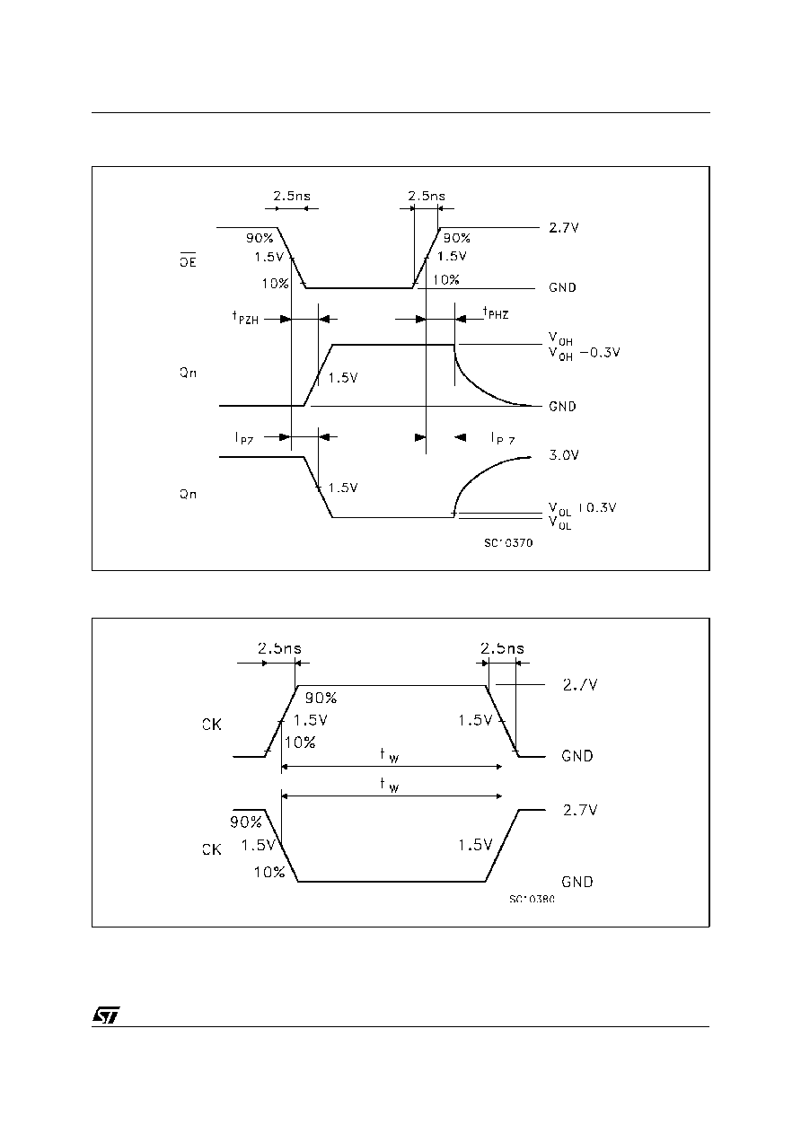
WAVEFORM 2: OUTPUT ENABLE AND DISABLE TIMES (f=1MHz; 50% duty cicle)
WAVEFORM 3: PULSE WIDTH
74LCX374
7/10

DIM.
mm
inch
MIN.
TYP.
MAX.
MIN.
TYP.
MAX.
A
2.65
0.104
a1
0.10
0.20
0.004
0.007
a2
2.45
0.096
b
0.35
0.49
0.013
0.019
b1
0.23
0.32
0.009
0.012
C
0.50
0.020
c1
45 (typ.)
D
12.60
13.00
0.496
0.512
E
10.00
10.65
0.393
0.419
e
1.27
0.050
e3
11.43
0.450
F
7.40
7.60
0.291
0.299
L
0.50
1.27
0.19
0.050
M
0.75
0.029
S
8 (max.)
P013L
SO-20 MECHANICAL DATA
74LCX374
8/10
DIM.
mm
inch
MIN.
TYP.
MAX.
MIN.
TYP.
MAX.
A
1.1
0.433
A1
0.05
0.10
0.15
0.002
0.004
0.006
A2
0.85
0.9
0.95
0.335
0.354
0.374
b
0.19
0.30
0.0075
0.0118
c
0.09
0.2
0.0035
0.0079
D
6.4
6.5
6.6
0.252
0.256
0.260
E
6.25
6.4
6.5
0.246
0.252
0.256
E1
4.3
4.4
4.48
0.169
0.173
0.176
e
0.65 BSC
0.0256 BSC
K
0
o
4
o
8
o
0
o
4
o
8
o
L
0.50
0.60
0.70
0.020
0.024
0.028
c
E
b
A2
A
E1
D
1
PIN 1 IDENTIFICATION
A1
L
K
e
TSSOP20 MECHANICAL DATA
74LCX374
9/10

Information furnished is believed to be accurate and reliable. However, STMicroelectronics assumes no responsibility for the consequences
of use of such information nor for any infringement of patents or other rights of third parties which may result from its use. No license is
granted by implication or otherwise under any patent or patent rights of STMicroelectronics. Specification mentioned in this publication are
subject to change without notice. This publication supersedes and replaces all information previously supplied. STMicroelectronics products
are not authorized for use as critical components in life support devices or systems without express written approval of STMicroelectronics.
The ST logo is a trademark of STMicroelectronics
©
1999 STMicroelectronics ≠ Printed in Italy ≠ All Rights Reserved
STMicroelectronics GROUP OF COMPANIES
Australia - Brazil - Canada - China - France - Germany - Italy - Japan - Korea - Malaysia - Malta - Mexico - Morocco - The Netherlands -
Singapore - Spain - Sweden - Switzerland - Taiwan - Thailand - United Kingdom - U.S.A.
http://www.st.com
.
74LCX374
10/10