1/13
September 2001
s
5V TOLERANT INPUTS AND OUTPUTS
s
HIGH SPEED :
t
PD
= 7.0 ns (MAX.) at V
CC
= 3V
s
POWER DOWN PROTECTION ON INPUTS
AND OUTPUTS
s
SYMMETRICAL OUTPUT IMPEDANCE:
|I
OH
| = I
OL
= 24mA (MIN) at V
CC
= 3V
s
PCI BUS LEVELS GUARANTEED AT 24 mA
s
BALANCED PROPAGATION DELAYS:
t
PLH
t
PHL
s
OPERATING VOLTAGE RANGE:
V
CC
(OPR) = 2.0V to 3.6V (1.5V Data
Retention)
s
PIN AND FUNCTION COMPATIBLE WITH
74 SERIES 646
s
LATCH-UP PERFORMANCE EXCEEDS
500mA (JESD 17)
s
ESD PERFORMANCE:
HBM > 2000V (MIL STD 883 method 3015);
MM > 200V
DESCRIPTION
The 74LCX646 is a low voltage CMOS OCTAL
BUS TRANSCEIVER AND REGISTER
(3-STATE) fabricated with sub-micron silicon gate
and double-layer metal wiring C
2
MOS technology.
It is ideal for low power and high speed 3.3V
applications; it can be interfaced to 5V signal
environment for both inputs and outputs.
This device consists of bus transceiver circuits
with 3 state, D-type flip-flops, and control circuitry
arranged for multiplexed transmission of data
directly from the input bus or from the internal
registers. Data on the A or B bus will be clocked
into register on the low to high transition of the
appropriate clock pin (Clock AB or Clock BA).
Enable (G) and direction (DIR) pins are provided
to control the transceiver functions. In the
transceiver mode, data present at the
high-impedance port may be stored in either
register or in both. The select controls (Select AB
select BA) can multiplex stored and real time
(transparent mode) data. The direction control
determines which bus will receive data when
enable G is active (low). In the isolation mode
74LCX646
LOW VOLT. CMOS OCTAL BUS TRANSCEIVER/REGISTER
WITH 5 VOLT TOLERANT INPUTS AND OUTPUTS(3-STATE)
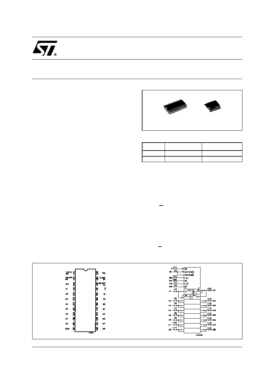
PIN CONNECTION AND IEC LOGIC SYMBOLS
ORDER CODES
PACKAGE
TUBE
T & R
SOP
74LCX646M1R
74LCX646RM13TR
TSSOP
74LCX646TTR
TSSOP
SOP
M74LCX646
2/13
(enable G high), "A" data may be stored in one
register and/or "B" data may be stored in the other
register. When an output function is disabled, the
input function is still enabled and may be used to
store and transmit data. Only one of the two
buses, A or B, may be driven at a time. It has
same speed performance at 3.3V than 5V
AC/ACT family, combined with a lower power
consumption.
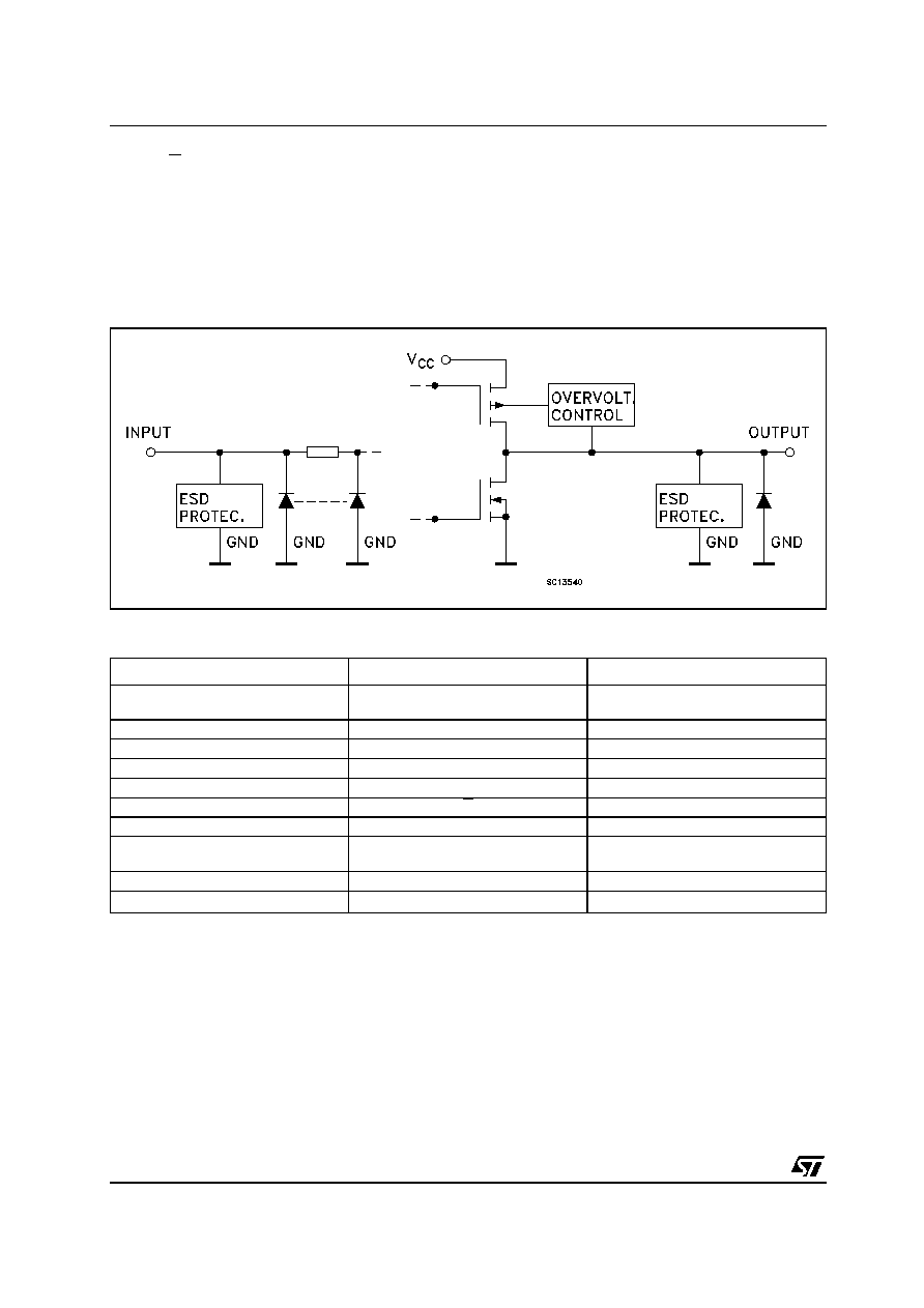
All inputs and outputs are equipped with
protection circuits against static discharge, giving
them 2KV ESD immunity and transient excess
voltage.
INPUT AND OUTPUT EQUIVALENT CIRCUIT
PIN DESCRIPTION
PIN No
SYMBOL
NAME AND FUNCTION
1
CLOCK AB (CAB)
A to B Clock Input (LOW to HIGH,
Edge-Triggered)
2
SELECT AB (SAB)
Select A to B Source Input
3
DIR
Direction Control Input
4, 5, 6, 7, 8, 9, 10, 11
A1 to A8
A Data Inputs/Outputs
20, 19, 18, 17, 16, 15, 14, 13
B1 to B8
B Data Inputs/Outputs
21
G
Output Enable Input (Active LOW)
22
SELECT BA (SBA)
Select B to A Source Input
23
CLOCK BA (CBA)
B to A Clock Input (LOW to HIGH,
Edge Triggered)
12
GND
Ground (0V)
24
V
CC
Positive Supply Voltage
M74LCX646
3/13
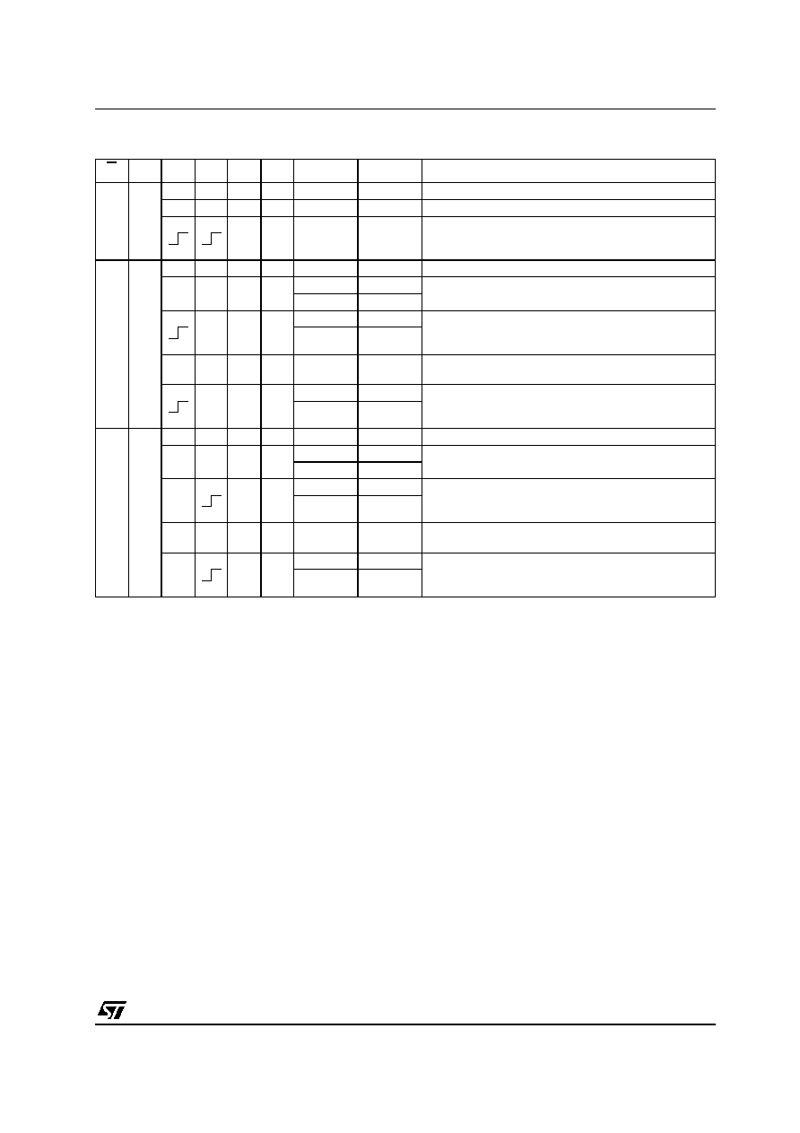
TRUTH TABLE
X : Don't Care
Z : High Impedance
Qn : The data stored to the internal flip-flops by most recent low to high transition of the clock inputs
* : The data at the A and B bus will be stored to the internal flip-flops on every low to high transition of the clock inputs.
G
DIR CAB CBA SAB SBA
A
B
FUNCTION
H
X
INPUTS
INPUTS
Both the A bus and the B bus are inputs
X
X
X
X
Z
Z
The Output functions of the A and B bus are disabled
X
X
INPUTS
INPUTS
Both the A and B bus are used as inputs to the internal
flip-flops. Data at the bus will be stored on low to high
transition of the clock inputs.
L
H
INPUTS
OUTPUTS The A bus are inputs and the B bus are outputs
X
X*
L
X
L
L
The data at the A bus are displayed at the B bus
H
H
X*
L
X
L
L
The data at the A bus are displayed at the B bus. The
data of the A bus are stored to internal flip-flop on low
to high transition of the clock pulse
H
H
X
X*
H
X
X
Qn
The data stored to the internal flip-flop are displayed at
the B bus.
X*
H
X
L
L
The data at the A bus are stored to the internal flip-flop
on low to high transition of the clock pulse. The states
of the internal flip-flops output directly to the B bus.
H
H
L
L
OUTPUTS
INPUTS
The B bus are inputs and the A bus are outputs.
X*
X
X
L
L
L
The data at the B bus are displayed at the A bus
H
H
X*
X
L
L
L
The data at the B bus are displayed at the A bus. The
data of the B bus are stored to the internal flip-flop on
low to high transition of the clock pulse.
H
H
X*
X
X
H
Qn
X
The data stored to the internal flip-flops are displayed
at the A bus
X*
X
H
L
L
The data at the B bus are stored to the internal flip-flop
on low to high transition of the clock pulse. The states
of the internal flip-flops output directly to the A bus.
H
H
M74LCX646
4/13
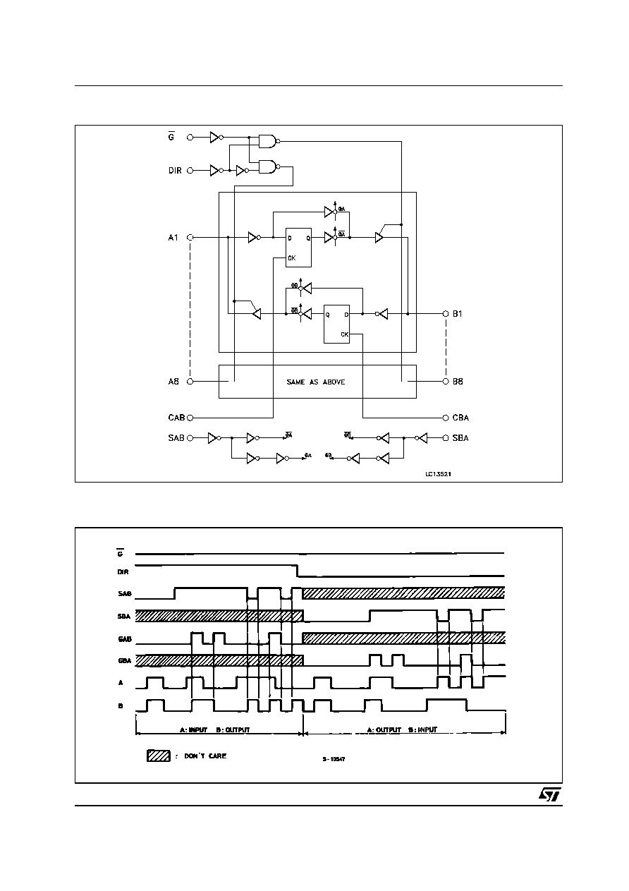
LOGIC DIAGRAM
This logic diagram has not be used to estimate propagation delays
TIMING CHART
M74LCX646
5/13
ABSOLUTE MAXIMUM RATINGS
Absolute Maximum Ratings are those values beyond which damage to the device may occur. Functional operation under these conditions is
not implied
1) I
O
absolute maximum rating must be observed
2) V
O
< GND
RECOMMENDED OPERATING CONDITIONS
1) Truth Table guaranteed: 1.5V to 3.6V
2) V
IN
from 0.8V to 2V at V
CC
= 3.0V
Symbol
Parameter
Value
Unit
V
CC
Supply Voltage
-0.5 to +7.0
V
V
I
DC Input Voltage
-0.5 to +7.0
V
V
O
DC Output Voltage (OFF State)
-0.5 to +7.0
V
V
O
DC Output Voltage (High or Low State) (note 1)
-0.5 to V
CC
+ 0.5
V
I
IK
DC Input Diode Current
- 50
mA
I
OK
DC Output Diode Current (note 2)
- 50
mA
I
O
DC Output Current
±
50
mA
I
CC
DC Supply Current per Supply Pin
±
100
mA
I
GND
DC Ground Current per Supply Pin
±
100
mA
T
stg
Storage Temperature
-65 to +150
∞C
T
L
Lead Temperature (10 sec)
300
∞C
Symbol
Parameter
Value
Unit
V
CC
Supply Voltage (note 1)
2.0 to 3.6
V
V
I
Input Voltage
0 to 5.5
V
V
O
Output Voltage (OFF State)
0 to 5.5
V
V
O
Output Voltage (High or Low State)
0 to V
CC
V
I
OH
, I
OL
High or Low Level Output Current (V
CC
= 3.0 to 3.6V)
±
24
mA
I
OH
, I
OL
High or Low Level Output Current (V
CC
= 2.7V)
±
12
mA
T
op
Operating Temperature
-55 to 125
∞C
dt/dv
Input Rise and Fall Time (note 2)
0 to 10
ns/V
M74LCX646
6/13
DC SPECIFICATIONS
DYNAMIC SWITCHING CHARACTERISTICS
1) Number of outputs defined as "n". Measured with "n-1" outputs switching from HIGH to LOW or LOW to HIGH. The remaining output is
measured in the LOW state.
Symbol
Parameter
Test Condition
Value
Unit
V
CC
(V)
-40 to 85 ∞C
-55 to 125 ∞C
Min.
Max.
Min.
Max.
V
IH
High Level Input
Voltage
2.7 to 3.6
2.0
2.0
V
V
IL
Low Level Input
Voltage
0.8
0.8
V
V
OH
High Level Output
Voltage
2.7 to 3.6
I
O
=-100
µ
A
V
CC
-0.2
V
CC
-0.2
V
2.7
I
O
=-12 mA
2.2
2.2
3.0
I
O
=-18 mA
2.4
2.4
I
O
=-24 mA
2.2
2.2
V
OL
Low Level Output
Voltage
2.7 to 3.6
I
O
=100
µ
A
0.2
0.2
V
2.7
I
O
=12 mA
0.4
0.4
3.0
I
O
=16 mA
0.4
0.4
I
O
=24 mA
0.55
0.55
I
I
Input Leakage
Current
2.7 to 3.6
V
I
= 0 to 5.5V
±
5
±
5
µ
A
I
off
Power Off Leakage
Current
0
V
I
or V
O
= 5.5V
10
10
µ
A
I
OZ
High Impedance
Output Leakage
Current
2.7 to 3.6
V
I
= V
IH
or V
IL
V
O
= 0 to V
CC
±
5
±
5
µ
A
I
CC
Quiescent Supply
Current
2.7 to 3.6
V
I
= V
CC
or GND
10
10
µ
A
V
I
or V
O
= 3.6 to 5.5V
±
10
±
10
I
CC
I
CC
incr. per Input
2.7 to 3.6
V
IH
= V
CC
- 0.6V
500
500
µ
A
Symbol
Parameter
Test Condition
Value
Unit
V
CC
(V)
T
A
= 25 ∞C
Min.
Typ.
Max.
V
OLP
Dynamic Low Level Quiet
Output (note 1)
3.3
C
L
= 50pF
V
IL
= 0V, V
IH
= 3.3V
0.8
V
V
OLV
-0.8
M74LCX646
7/13
AC ELECTRICAL CHARACTERISTICS
1) Skew is defined as the absolute value of the difference between the actual propagation delay for any two outputs of the same device switch-
ing in the same direction, either HIGH or LOW (t
OSLH
= | t
PLHm
- t
PLHn
|, t
OSHL
= | t
PHLm
- t
PHLn
|)
2) Parameter guaranteed by design
CAPACITIVE CHARACTERISTICS
1) C
PD
is defined as the value of the IC's internal equivalent capacitance which is calculated from the operating current consumption without
load. (Refer to Test Circuit). Average operating current can be obtained by the following equation. I
CC(opr)
= C
PD
x V
CC
x f
IN
+ I
CC
/8 (per circuit)
Symbol
Parameter
Test Condition
Value
Unit
V
CC
(V)
C
L
(pF)
R
L
(
)
t
s
= t
r
(ns)
-40 to 85 ∞C
-55 to 125 ∞C
Min.
Max.
Min.
Max.
t
PLH
t
PHL
Propagation Delay
Time (CAB or CBA
to An or Bn)
2.7
50
500
2.5
1.5
9.5
1.5
9.5
ns
3.0 to 3.6
1.5
8.5
1.5
8.5
t
PLH
t
PHL
Propagation Delay
Time (An to Bn or Bn
to An)
2.7
50
500
2.5
1.5
8.0
1.5
8.0
ns
3.0 to 3.6
1.5
7.0
1.5
7.0
t
PLH
t
PHL
Propagation Delay
Time (SAB or SBA
to An or Bn)
2.7
50
500
2.5
1.5
9.5
1.5
9.5
ns
3.0 to 3.6
1.5
8.5
1.5
8.5
t
PZL
t
PZH
Output Enable Time
(G, DIR to An, Bn)
2.7
50
500
2.5
1.5
9.5
1.5
9.5
ns
3.0 to 3.6
1.5
8.5
1.5
8.5
t
PLZ
t
PHZ
Output Disable Time
(G, DIR to An, Bn)
2.7
50
500
2.5
1.5
9.5
1.5
9.5
ns
3.0 to 3.6
1.5
8.5
1.5
8.5
t
S
Setup Time, HIGH or
LOW level Data to
CAB, CBA
2.7
50
500
2.5
2.5
2.5
ns
3.0 to 3.6
2.5
2.5
t
h
Hold Time, HIGH or
LOW level Data to
CAB, CBA
2.7
50
500
2.5
1.5
1.5
ns
3.0 to 3.6
1.5
1.5
t
W
CAB, CBA Pulse
Width, HIGH or
LOW
2.7
50
500
2.5
4.0
4.0
ns
3.0 to 3.6
3.3
3.3
f
MAX
Clock Pulse
Frequency
3.0 to 3.6
50
500
2.5
150
150
MHz
t
OSLH
t
OSHL
Output To Output
Skew Time (note1,
2)
3.0 to 3.6
50
500
2.5
1.0
1.0
ns
Symbol
Parameter
Test Condition
Value
Unit
V
CC
(V)
T
A
= 25 ∞C
Min.
Typ.
Max.
C
IN
Input Capacitance
3.3
V
IN
= 0 to V
CC
6
pF
C
I/O
I/O Capacitance
3.3
V
IN
= 0 to V
CC
10
pF
C
PD
Power Dissipation Capacitance
(note 1)
3.3
f
IN
= 10MHz
V
IN
= 0 or V
CC
37
pF

M74LCX646
8/13
TEST CIRCUIT
C
L
= 50 pF or equivalent (includes jig and probe capacitance)
R
L
= R1 = 500
or equivalent
R
T
= Z
OUT
of pulse generator (typically 50
)
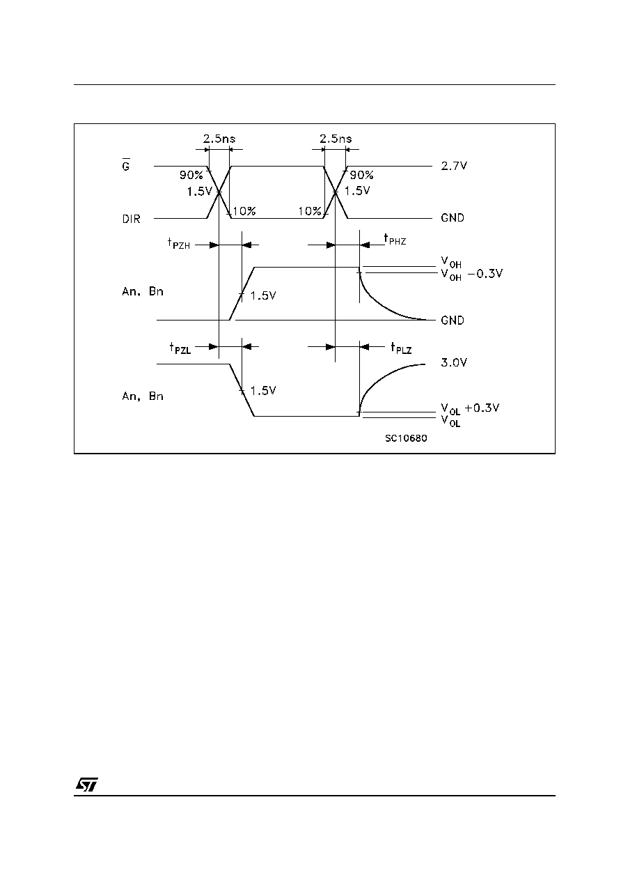
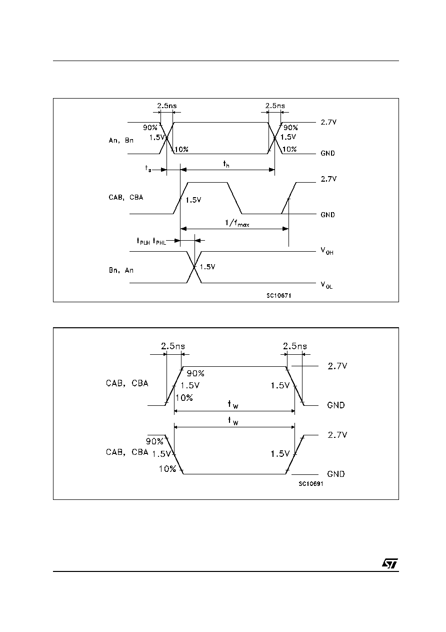
WAVEFORM 1 : PROPAGATION DELAYS, SAB, SBA, An, Bn, TIMES (f=1MHz; 50% duty cycle)
TEST
SWITCH
t
PLH
, t
PHL
Open
t
PZL
, t
PLZ
6V
t
PZH
, t
PHZ
GND
M74LCX646
9/13
WAVEFORM 2 : OUTPUT ENABLE AND DISABLE TIME (f=1MHz; 50% duty cycle)
M74LCX646
10/13
WAVEFORM 3 : SETUP AND HOLD TIME, CAB, CBA MAXIMUM FREQUENCY (f=1MHz; 50% duty
cycle)
WAVEFORM 4 : PULSE WIDTH (f=1MHz; 50% duty cycle)
M74LCX646
11/13
DIM.
mm.
inch
MIN.
TYP
MAX.
MIN.
TYP.
MAX.
A
2.65
0.104
a1
0.1
0.2
0.004
0.008
a2
2.45
0.096
b
0.35
0.49
0.014
0.019
b1
0.23
0.32
0.009
0.012
C
0.5
0.020
c1
45∞ (typ.)
D
15.20
15.60
0.598
0.614
E
10.00
10.65
0.393
0.419
e
1.27
0.050
e3
13.97
0.550
F
7.40
7.60
0.291
0.300
L
0.50
1.27
0.020
0.050
S
8∞ (max.)
SO-24 MECHANICAL DATA
PO13T
F
C
L
E
a1
b1
A
e
D
e3
b
24
13
1
12
c1
s
a2
M74LCX646
12/13
DIM.
mm.
inch
MIN.
TYP
MAX.
MIN.
TYP.
MAX.
A
1.1
0.043
A1
0.05
0.15
0.002
0.006
A2
0.9
0.035
b
0.19
0.30
0.0075
0.0118
c
0.09
0.20
0.0035
0.0079
D
7.7
7.9
0.303
0.311
E
6.25
6.5
0.246
0.256
E1
4.3
4.5
0.169
0.177
e
0.65 BSC
0.0256 BSC
K
0∞
8∞
0∞
8∞
L
0.50
0.70
0.020
0.028
TSSOP24 MECHANICAL DATA
c
E
b
A2
A
E1
D
1
PIN 1 IDENTIFICATION
A1
L
K
e
7047476A

M74LCX646
Information furnished is believed to be accurate and reliable. However, STMicroelectronics assumes no responsibility for the
consequences of use of such information nor for any infringement of patents or other rights of third parties which may result from
its use. No license is granted by implication or otherwise under any patent or patent rights of STMicroelectronics. Specifications
mentioned in this publication are subject to change without notice. This publication supersedes and replaces all information
previously supplied. STMicroelectronics products are not authorized for use as critical components in life support devices or
systems without express written approval of STMicroelectronics.
© The ST logo is a registered trademark of STMicroelectronics
© 2001 STMicroelectronics - Printed in Italy - All Rights Reserved
STMicroelectronics GROUP OF COMPANIES
Australia - Brazil - China - Finland - France - Germany - Hong Kong - India - Italy - Japan - Malaysia - Malta - Morocco
Singapore - Spain - Sweden - Switzerland - United Kingdom
© http://www.st.com
13/13