 | –≠–ª–µ–∫—Ç—Ä–æ–Ω–Ω—ã–π –∫–æ–º–ø–æ–Ω–µ–Ω—Ç: 74LVQ10 | –°–∫–∞—á–∞—Ç—å:  PDF PDF  ZIP ZIP |

1/11
July 2004
s
HIGH SPEED:
t
PD
= 5.3ns (TYP.) at V
CC
= 3.3 V
s
COMPATIBLE WITH TTL OUTPUTS
s
LOW POWER DISSIPATION:
I
CC
= 2
µ
A (MAX.) at T
A
=25∞C
s
LOW NOISE:
V
OLP
= 0.3V (TYP.) at V
CC
= 3.3V
s
75
TRANSMISSION LINE DRIVING
CAPABILITY
s
SYMMETRICAL OUTPUT IMPEDANCE:
|I
OH
| = I
OL
= 12mA (MIN) at V
CC
= 3.0 V
s
PCI BUS LEVELS GUARANTEED AT 24 mA
s
BALANCED PROPAGATION DELAYS:
t
PLH
t
PHL
s
OPERATING VOLTAGE RANGE:
V
CC
(OPR) = 2V to 3.6V (1.2V Data Retention)
s
PIN AND FUNCTION COMPATIBLE WITH
74 SERIES 10
s
IMPROVED LATCH-UP IMMUNITY
DESCRIPTION
The 74LVQ10 is a low voltage CMOS TRIPLE
3-INPUT NAND GATE fabricated with sub-micron
silicon gate and double-layer metal wiring C
2
MOS
technology. It is ideal for low power and low noise
3.3V applications.
The internal circuit is composed of 3 stages
including buffer output, which enables high noise
immunity and stable output.
All inputs and outputs are equipped with
protection circuits against static discharge, giving
them 2KV ESD immunity and transient excess
voltage.
74LVQ10
TRIPLE 3-INPUT NAND GATE
Figure 1: Pin Connection And IEC Logic Symbols
Table 1: Order Codes
PACKAGE
T & R
SOP
74LVQ10MTR
TSSOP
74LVQ10TTR
TSSOP
SOP
Rev. 2

74LVQ10
2/11
Figure 2: Input And Output Equivalent Circuit
Table 2: Pin Description
Table 3: Truth Table
Table 4: Absolute Maximum Ratings
Absolute Maximum Ratings are those values beyond which damage to the device may occur. Functional operation under these conditions is
not implied
Table 5: Recommended Operating Conditions
1) Truth Table guaranteed: 1.2V to 3.6V
2) V
IN
from 0.8V to 2V
PIN N∞
SYMBOL
NAME AND FUNCTION
1, 3, 9
1A to 3A
Data Inputs
2, 4, 10
1B to 3B
Data Inputs
13, 5, 11
1C to 3C
Data Inputs
12, 6, 8
1Y to 3Y
Data Outputs
7
GND
Ground (0V)
14
V
CC
Positive Supply Voltage
A
B
C
Y
L
X
X
H
X
L
X
H
X
X
L
H
H
H
H
L
Symbol
Parameter
Value
Unit
V
CC
Supply Voltage
-0.5 to +7
V
V
I
DC Input Voltage
-0.5 to V
CC
+ 0.5
V
V
O
DC Output Voltage
-0.5 to V
CC
+ 0.5
V
I
IK
DC Input Diode Current
±
20
mA
I
OK
DC Output Diode Current
±
20
mA
I
O
DC Output Current
±
50
mA
I
CC
or I
GND
DC V
CC
or Ground Current
±
150
mA
T
stg
Storage Temperature
-65 to +150
∞C
T
L
Lead Temperature (10 sec)
300
∞C
Symbol
Parameter
Value
Unit
V
CC
Supply Voltage (note 1)
2 to 3.6
V
V
I
Input Voltage
0 to V
CC
V
V
O
Output Voltage
0 to V
CC
V
T
op
Operating Temperature
-55 to 125
∞C
dt/dv
Input Rise and Fall Time V
CC
= 3.0V (note 2)
0 to 10
ns/V

74LVQ10
3/11
Table 6: DC Specifications
1) Maximum test duration 2ms, one output loaded at time
2) Incident wave switching is guaranteed on transmission lines with impedances as low as 75
Table 7: Dynamic Switching Characteristics
1) Worst case package.
2) Max number of outputs defined as (n). Data inputs are driven 0V to 3.3V, (n-1) outputs switching and one output at GND.
3) Max number of data inputs (n) switching. (n-1) switching 0V to 3.3V. Inputs under test switching: 3.3V to threshold (V
ILD
), 0V to threshold
(V
IHD
), f=1MHz.
Symbol
Parameter
Test Condition
Value
Unit
V
CC
(V)
T
A
= 25∞C
-40 to 85∞C
-55 to 125∞C
Min.
Typ.
Max.
Min.
Max.
Min.
Max.
V
IH
High Level Input
Voltage
3.0 to
3.6
2.0
2.0
2.0
V
V
IL
Low Level Input
Voltage
0.8
0.8
0.8
V
V
OH
High Level Output
Voltage
3.0
I
O
=-50
µ
A
2.9
2.99
2.9
2.9
V
I
O
=-12 mA
2.58
2.48
2.48
I
O
=-24 mA
2.2
2.2
V
OL
Low Level Output
Voltage
3.0
I
O
=50
µ
A
0.002
0.1
0.1
0.1
V
I
O
=12 mA
0
0.36
0.44
0.44
I
O
=24 mA
0.55
0.55
I
I
Input Leakage
Current
3.6
V
I
= V
CC
or GND
±
0.1
±
1
±
1
µ
A
I
CC
Quiescent Supply
Current
3.6
V
I
= V
CC
or GND
2
20
20
µ
A
I
OLD
Dynamic Output
Current (note 1, 2)
3.6
V
OLD
= 0.8 V max
36
25
mA
I
OHD
V
OHD
= 2 V min
-25
-25
mA
Symbol
Parameter
Test Condition
Value
Unit
V
CC
(V)
T
A
= 25∞C
-40 to 85∞C
-55 to 125∞C
Min.
Typ.
Max.
Min.
Max.
Min.
Max.
V
OLP
Dynamic Low
Voltage Quiet
Output (note 1, 2)
3.3
C
L
= 50 pF
0.3
0.8
V
V
OLV
-0.8
-0.3
V
IHD
Dynamic High
Voltage Input (note
1, 3)
3.3
2
V
V
ILD
Dynamic Low
Voltage Input (note
1, 3)
3.3
0.8
V

74LVQ10
4/11
Table 8: AC Electrical Characteristics (C
L
= 50 pF, R
L
= 500
, Input t
r
= t
f
= 3ns)
1) Skew is defined as the absolute value of the difference between the actual propagation delay for any two outputs of the same device switch-
ing in the same direction, either HIGH or LOW (t
OSLH
= |t
PLHm
- t
PLHn
|, t
OSHL
= |t
PHLm
- t
PHLn
|)
2) Parameter guaranteed by design
(*) Voltage range is 3.3V
±
0.3V
Table 9: Capacitive Characteristics
1) C
PD
is defined as the value of the IC's internal equivalent capacitance which is calculated from the operating current consumption without
load. (Refer to Test Circuit). Average operating current can be obtained by the following equation. I
CC(opr)
= C
PD
x V
CC
x f
IN
+ I
CC
/n (per circuit)
Figure 3: Test Circuit
C
L
= 50pF or equivalent (includes jig and probe capacitance)
R
L
= 500
or equivalent
R
T
= Z
OUT
of pulse generator (typically 50
)
Symbol
Parameter
Test Condition
Value
Unit
V
CC
(V)
T
A
= 25∞C
-40 to 85∞C
-55 to 125∞C
Min.
Typ.
Max.
Min.
Max.
Min.
Max.
t
PLH
t
PHL
Propagation Delay
Time
2.7
.
6.0
10.0
11.5
13.0
ns
3.3
(*)
5.3
8.0
9.0
10.5
t
OSLH
t
OSHL
Output To Output
Skew Time
(note1, 2)
2.7
0.5
1.0
1.0
1.0
ns
3.3
(*)
0.5
1.0
1.0
1.0
Symbol
Parameter
Test Condition
Value
Unit
V
CC
(V)
T
A
= 25∞C
-40 to 85∞C
-55 to 125∞C
Min.
Typ.
Max.
Min.
Max.
Min.
Max.
C
IN
Input Capacitance
3.3
4
pF
C
PD
Power Dissipation
Capacitance (note
1)
3.3
f
IN
= 10MHz
30
pF

74LVQ10
5/11
Figure 4: Waveform - Propagation Delays (f=1MHz; 50% duty cycle)
74LVQ10
6/11
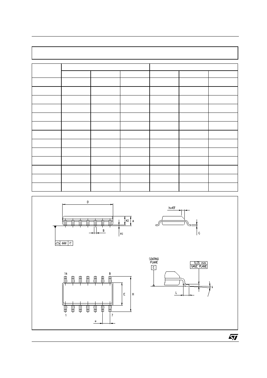
DIM.
mm.
inch
MIN.
TYP
MAX.
MIN.
TYP.
MAX.
A
1.35
1.75
0.053
0.069
A1
0.1
0.25
0.004
0.010
A2
1.10
1.65
0.043
0.065
B
0.33
0.51
0.013
0.020
C
0.19
0.25
0.007
0.010
D
8.55
8.75
0.337
0.344
E
3.8
4.0
0.150
0.157
e
1.27
0.050
H
5.8
6.2
0.228
0.244
h
0.25
0.50
0.010
0.020
L
0.4
1.27
0.016
0.050
k
0∞
8∞
0∞
8∞
ddd
0.100
0.004
SO-14 MECHANICAL DATA
0016019D
74LVQ10
7/11
DIM.
mm.
inch
MIN.
TYP
MAX.
MIN.
TYP.
MAX.
A
1.2
0.047
A1
0.05
0.15
0.002
0.004
0.006
A2
0.8
1
1.05
0.031
0.039
0.041
b
0.19
0.30
0.007
0.012
c
0.09
0.20
0.004
0.0089
D
4.9
5
5.1
0.193
0.197
0.201
E
6.2
6.4
6.6
0.244
0.252
0.260
E1
4.3
4.4
4.48
0.169
0.173
0.176
e
0.65 BSC
0.0256 BSC
K
0∞
8∞
0∞
8∞
L
0.45
0.60
0.75
0.018
0.024
0.030
TSSOP14 MECHANICAL DATA
c
E
b
A2
A
E1
D
1
PIN 1 IDENTIFICATION
A1
L
K
e
0080337D

74LVQ10
8/11
DIM.
mm.
inch
MIN.
TYP
MAX.
MIN.
TYP.
MAX.
A
330
12.992
C
12.8
13.2
0.504
0.519
D
20.2
0.795
N
60
2.362
T
22.4
0.882
Ao
6.4
6.6
0.252
0.260
Bo
9
9.2
0.354
0.362
Ko
2.1
2.3
0.082
0.090
Po
3.9
4.1
0.153
0.161
P
7.9
8.1
0.311
0.319
Tape & Reel SO-14 MECHANICAL DATA
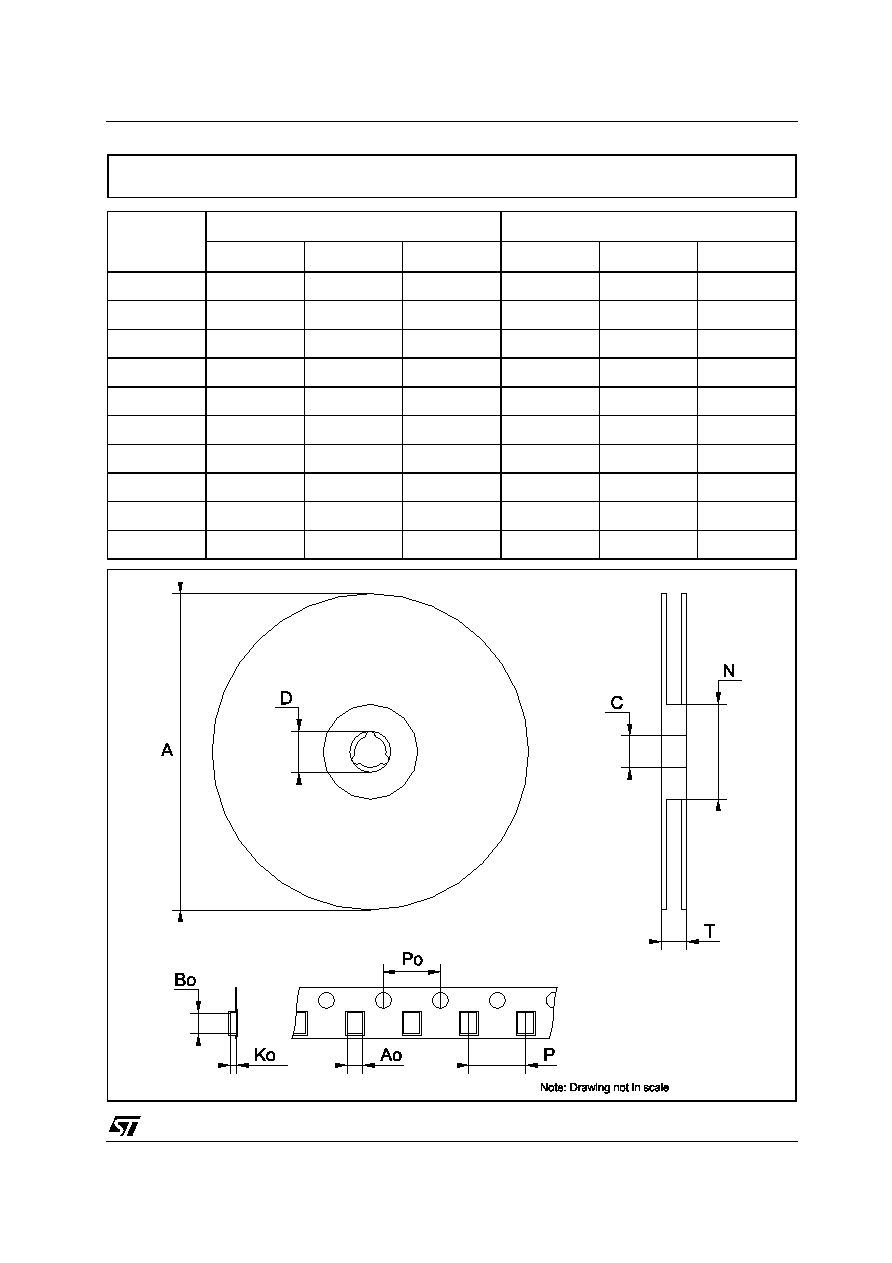
74LVQ10
9/11
DIM.
mm.
inch
MIN.
TYP
MAX.
MIN.
TYP.
MAX.
A
330
12.992
C
12.8
13.2
0.504
0.519
D
20.2
0.795
N
60
2.362
T
22.4
0.882
Ao
6.7
6.9
0.264
0.272
Bo
5.3
5.5
0.209
0.217
Ko
1.6
1.8
0.063
0.071
Po
3.9
4.1
0.153
0.161
P
7.9
8.1
0.311
0.319
Tape & Reel TSSOP14 MECHANICAL DATA
74LVQ10
10/11
Table 10: Revision History
Date
Revision
Description of Changes
29-Jul-2004
2
Ordering Codes Revision - pag. 1.

74LVQ10
11/11
Information furnished is believed to be accurate and reliable. However, STMicroelectronics assumes no responsibility for the consequences
of use of such information nor for any infringement of patents or other rights of third parties which may result from its use. No license is granted
by implication or otherwise under any patent or patent rights of STMicroelectronics. Specifications mentioned in this publication are subject
to change without notice. This publication supersedes and replaces all information previously supplied. STMicroelectronics products are not
authorized for use as critical components in life support devices or systems without express written approval of STMicroelectronics.
The ST logo is a registered trademark of STMicroelectronics
All other names are the property of their respective owners
© 2004 STMicroelectronics - All Rights Reserved
STMicroelectronics group of companies
Australia - Belgium - Brazil - Canada - China - Czech Republic - Finland - France - Germany - Hong Kong - India - Israel - Italy - Japan -
Malaysia - Malta - Morocco - Singapore - Spain - Sweden - Switzerland - United Kingdom - United States of America
www.st.com