1/13
July 2001
s
HIGH SPEED:
f
MAX
= 180 MHz (TYP.) at V
CC
= 3.3 V
s
COMPATIBLE WITH TTL OUTPUTS
s
LOW POWER DISSIPATION:
I
CC
= 4
µ
A (MAX.) at T
A
=25∞C
s
LOW NOISE:
V
OLP
= 0.3V (TYP.) at V
CC
= 3.3V
s
75
TRANSMISSION LINE DRIVING
CAPABILITY
s
SYMMETRICAL OUTPUT IMPEDANCE:
|I
OH
| = I
OL
= 12mA (MIN) at V
CC
= 3.0 V
s
PCI BUS LEVELS GUARANTEED AT 24 mA
s
BALANCED PROPAGATION DELAYS:
t
PLH
t
PHL
s
OPERATING VOLTAGE RANGE:
V
CC
(OPR) = 2V to 3.6V (1.2V Data Retention)
s
PIN AND FUNCTION COMPATIBLE WITH
74 SERIES 161
s
IMPROVED LATCH-UP IMMUNITY
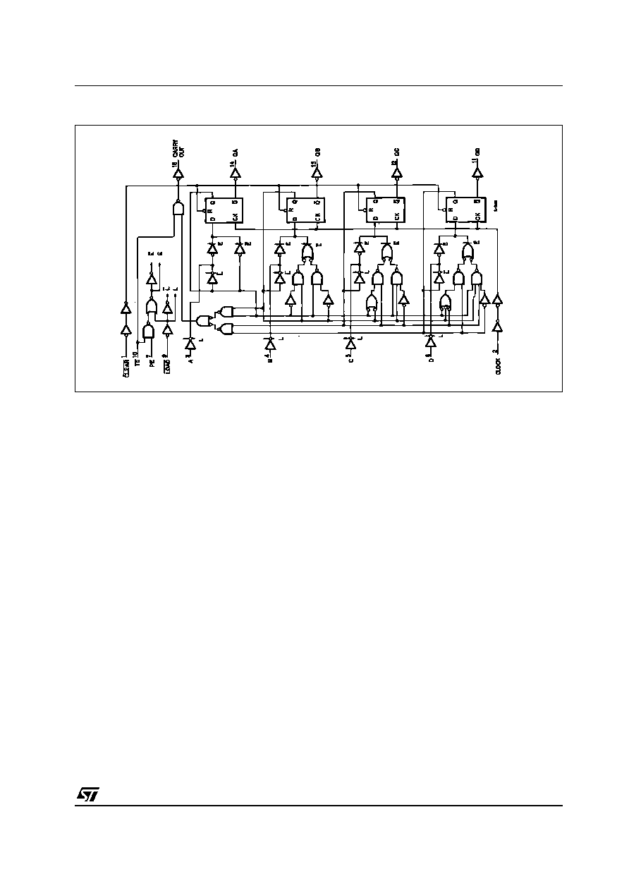
DESCRIPTION
The 74LVQ161 is a low voltage CMOS
SYNCHRONOUS PRESETTABLE COUNTER
fabricated with sub-micron silicon gate and
double-layer metal wiring C
2
MOS technology. It is
ideal for low power and low noise 3.3V
applications. It is a 4 bit binary counter with
Asynchronous Clear.
The circuit have four fundamental modes of
operation, in order of preference: synchronous
reset, parallel load, count-up and hold. Four
control inputs, Master Reset (CLEAR), Parallel
Enable Input (PE) and Count Enable Carry Input
(TE), determine the mode of operation as shown
in the Truth Table. A LOW signal on CLEAR
overrides counting and parallel loading and sets
all outputs on LOW state. A LOW signal on LOAD
overrides counting and allows information on
Parallel Data Qn inputs to be loaded into the
flip-flops on the next rising edge of CLOCK. With
LOAD and CLEAR, PE and TE permit counting
when both are high. Conversely, a LOW signal on
either PE and TE inhibits counting. All inputs and
outputs are equipped with protection circuits
against static discharge, giving them 2KV ESD
immunity and transient excess voltage.
74LVQ161
SYNCHRONOUS PRESETTABLE 4-BIT COUNTER
PIN CONNECTION AND IEC LOGIC SYMBOLS
ORDER CODES
PACKAGE
TUBE
T & R
SOP
74LVQ161M
74LVQ161MTR
TSSOP
74LVQ161TTR
TSSOP
SOP
74LVQ161
2/13
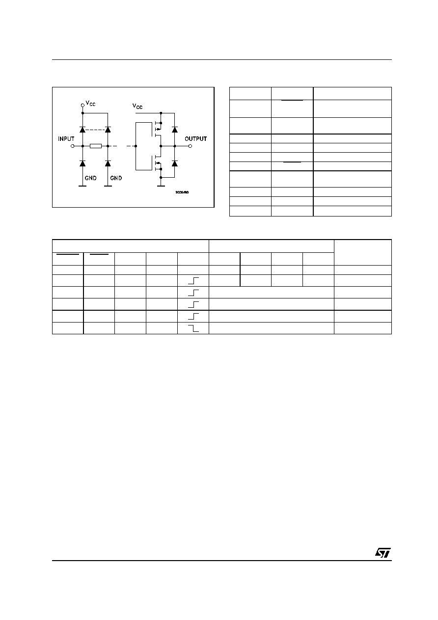
INPUT AND OUTPUT EQUIVALENT CIRCUIT
PIN DESCRIPTION
TRUTH TABLE
X : Don't Care; A, B, C, D; Logic level of data input; CARRY OUT : TE x QA x QB x QC x QD
PIN No
SYMBOL
NAME AND FUNCTION
1
CLEAR
Asynchronous
Master
Reset
2
CLOCK
Clock Input (LOW to
HIGH Edge Trigger)
3, 4, 5, 6
A, B, C, D
Data Inputs
7
PE
Count Enable Input
10
TE
Count Enable Carry Input
9
LOAD
Parallel Enable Input
14, 13, 12,
11
QA to QD
Flip-Flop Outputs
15
CARRY OUT Terminal Count Output
8
GND
Ground (0V)
16
V
CC
Positive Supply Voltage
INPUTS
OUTPUTS
FUNCTION
CLEAR
LOAD
PE
TE
CK
L
X
X
X
X
L
L
L
L
RESET TO "0"
H
L
X
X
A
B
C
D
PRESET DATA
H
H
X
L
NO CHANGE
NO COUNT
H
H
L
X
NO CHANGE
NO COUNT
H
H
H
H
COUNT UP
COUNT
H
X
X
X
NO CHANGE
NO COUNT
74LVQ161
4/13
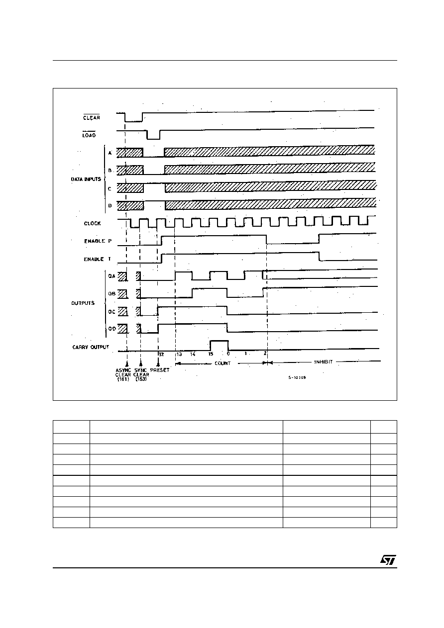
TIMING CHART
ABSOLUTE MAXIMUM RATINGS
Absolute Maximum Ratings are those values beyond which damage to the device may occur. Functional operation under these conditions is
not implied
Symbol
Parameter
Value
Unit
V
CC
Supply Voltage
-0.5 to +7
V
V
I
DC Input Voltage
-0.5 to V
CC
+ 0.5
V
V
O
DC Output Voltage
-0.5 to V
CC
+ 0.5
V
I
IK
DC Input Diode Current
±
20
mA
I
OK
DC Output Diode Current
±
20
mA
I
O
DC Output Current
±
50
mA
I
CC
or I
GND
DC V
CC
or Ground Current
±
300
mA
T
stg
Storage Temperature
-65 to +150
∞C
T
L
Lead Temperature (10 sec)
300
∞C
74LVQ161
5/13
RECOMMENDED OPERATING CONDITIONS
1) Truth Table guaranteed: 1.2V to 3.6V
2) V
IN
from 0.8V to 2V
DC SPECIFICATIONS
1) Maximum test duration 2ms, one output loaded at time
2) Incident wave switching is guaranteed on transmission lines with impedances as low as 75
Symbol
Parameter
Value
Unit
V
CC
Supply Voltage (note 1)
2 to 3.6
V
V
I
Input Voltage
0 to V
CC
V
V
O
Output Voltage
0 to V
CC
V
T
op
Operating Temperature
-55 to 125
∞C
dt/dv
Input Rise and Fall Time V
CC
= 3.0V (note 2)
0 to 10
ns/V
Symbol
Parameter
Test Condition
Value
Unit
V
CC
(V)
T
A
= 25∞C
-40 to 85∞C
-55 to 125∞C
Min.
Typ.
Max.
Min.
Max.
Min.
Max.
V
IH
High Level Input
Voltage
3.0 to
3.6
2.0
2.0
2.0
V
V
IL
Low Level Input
Voltage
0.8
0.8
0.8
V
V
OH
High Level Output
Voltage
3.0
I
O
=-50
µ
A
2.9
2.99
2.9
2.9
V
I
O
=-12 mA
2.58
2.48
2.48
I
O
=-24 mA
2.2
2.2
V
OL
Low Level Output
Voltage
3.0
I
O
=50
µ
A
0.002
0.1
0.1
0.1
V
I
O
=12 mA
0
0.36
0.44
0.44
I
O
=24 mA
0.55
0.55
I
I
Input Leakage
Current
3.6
V
I
= V
CC
or GND
±
0.1
±
1
±
1
µ
A
I
CC
Quiescent Supply
Current
3.6
V
I
= V
CC
or GND
4
40
40
µ
A
I
OLD
Dynamic Output
Current (note 1, 2)
3.6
V
OLD
= 0.8 V max
36
25
mA
I
OHD
V
OHD
= 2 V min
-25
-25
mA