1/11
May 2003
s
HIGH SPEED:
t
PD
= 0.4 ns (TYP.) at V
CC
= 3.3 V
t
PD
= 0.1 ns (TYP.) at V
CC
= 5 V
s
LOW POWER DISSIPATION:
I
CC
= 2
µ
A (MAX.) at T
A
=25∞C
s
LOW "ON " LOW RESISTANCE
R
ON
= 14
at V
CC
= 3.3V , I
I/O
<
1 mA
R
ON
= 12
at V
CC
= 5.0V , I
I/O
<
1 mA
s
SINE WAVE DISTORTION :
0.04% at V
CC
= 3.3V , f = 1KHz
s
OPERATING VOLTAGE RANGE:
V
CC(OPR)
= 2V to 5.5V
s
PIN AND FUNCTION COMPATIBLE WITH
74 SERIES 4066
s
IMPROVED LATCH-UP IMMUNITY
DESCRIPTION
The 74LVQ4066 is a low voltage CMOS QUAD
BILATERAL SWITCH fabricated with sub-micron
silicon gate and double-layer metal wiring C
2
MOS
technology.
It is ideal for low power and low noise 3.3V
applications and each switch is designed to
handle both analog and digital signals.
The switches permit signals with amplitudes up to
Vcc (peak) to be transmitted in either direction
without relevant propagation delay and without
generating additional ground bounce noise.
It has an ON-Resistance which is greatly reduced
in comparison with 74HC4066.
It is provided of four individual enable inputs to
control the switches; the switch is ON when the C
input is held high and OFF (High Impedance)
when C is held low.
All
inputs
and
outputs
are
equipped
with
protection circuits against static discharge, giving
them ESD immunity and transient excess voltage.
74LVQ4066
QUAD BILATERAL SWITCH
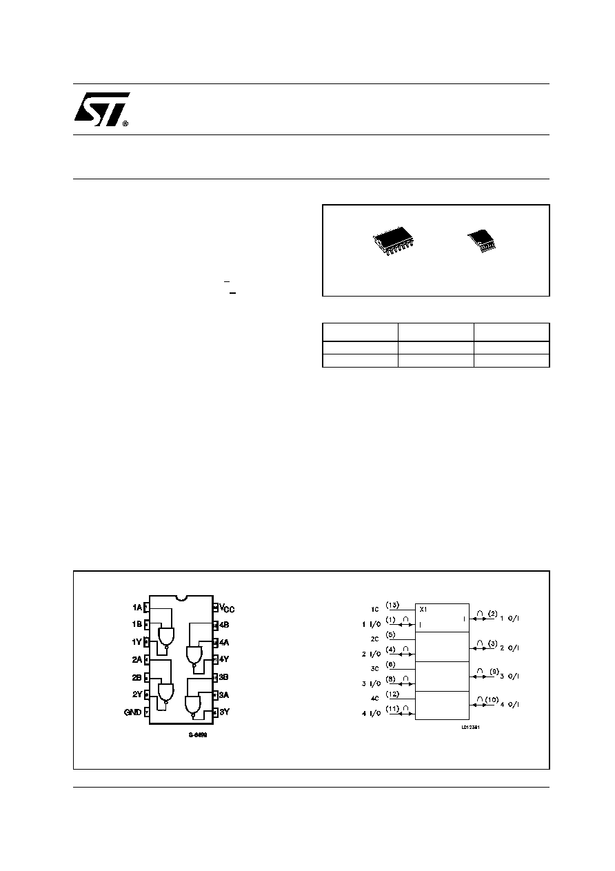
PIN CONNECTION AND IEC LOGIC SYMBOLS
ORDER CODES
PACKAGE
TUBE
T & R
SOP
74LVQ4066M
74LVQ4066MTR
TSSOP
74LVQ4066TTR
TSSOP
SOP
74LVQ4066
2/11
LOGIC DIAGRAM
PIN DESCRIPTION
TRUTH TABLE
(*) High Impedance
ABSOLUTE MAXIMUM RATINGS
Absolute Maximum Ratings are those values beyond which damage to the device may occur. Functional operation under these conditions is
not implied
RECOMMENDED OPERATING CONDITIONS
1) Truth Table guaranteed: 1.2V to 5.5V
2) V
IN
from 30% to 70%V
CC
PIN No
SYMBOL
NAME AND FUNCTION
1, 4, 8, 11
1 to 4 I/O
Independent Input/Output
2, 3, 9, 10
1 to 4 O/I
Independent Output/Input
13, 5, 6, 12
1C to 4C
Enable Input (Active
HIGH)
7
GND
Ground (0V)
14
V
CC
Positive Supply Voltage
A
B
H
ON
L
OFF*
Symbol
Parameter
Value
Unit
V
CC
Supply Voltage
-0.5 to +7
V
V
I
DC Input Voltage
-0.5 to V
CC
+ 0.5
V
V
O
DC Output Voltage
-0.5 to V
CC
+ 0.5
V
I
IK
DC Input Diode Current
±
20
mA
I
OK
DC Output Diode Current
±
20
mA
I
O
DC Output Current
±
50
mA
I
CC
or I
GND
DC V
CC
or Ground Current
±
200
mA
T
stg
Storage Temperature
-65 to +150
∞C
T
L
Lead Temperature (10 sec)
300
∞C
Symbol
Parameter
Value
Unit
V
CC
Supply Voltage (note 1)
2 to 5.5
V
V
I
Input Voltage
0 to V
CC
V
V
O
Output Voltage
0 to V
CC
V
T
op
Operating Temperature
-55 to 125
∞C
dt/dv
Input Rise and Fall Time on control pin V
CC
= 3.0V (note 2)
0 to 10
ns/V
74LVQ4066
3/11
DC SPECIFICATIONS
(*)Voltage range is 5V
±
0.5V
(**)Voltage range is 3.3V
±
0.3V
Symbol
Parameter
Test Condition
Value
Unit
V
CC
(V)
T
A
= 25∞C
-40 to 85∞C
-55 to 125∞C
Min.
Typ.
Max.
Min.
Max.
Min.
Max.
V
IH
High Level Input
Voltage
2.7 to
5.5
0.7
V
CC
0.7
V
CC
0.7
V
CC
V
V
IL
Low Level Input
Voltage
0.3
V
CC
0.3
V
CC
0.3
V
CC
V
R
ON
ON Resistance
3.3
(**)
V
I
=V
IH
V
I/O
=V
CC
to GND
I
I/O
< 1mA
16.5
23
32
40
5.0(*)
12
17
22
26
3.3
(**)
V
I
=V
IH
V
I/O
=V
CC
or GND
I
I/O
< 1mA
12
17
24
30
5.0(*)
9.5
13
17
20
R
ON
Difference of ON
Resistance
Between Switches
3.0 to
5.5
V
I
=V
IH
V
I/O
=V
CC
to GND
I
I/O
< 1mA
2
I
OFF
Input/Output
Leakage Current
(SWITCH OFF)
5.5
V
OS
= V
CC
to GND
V
IS
= V
CC
to GND
V
I
= V
IL
±
0.1
±
1.0
±
1.0
µ
A
I
IZ
Switch Input
Leakage Current
(SWITCH ON ,
OUTPUT OFF)
5.5
V
OS
= V
CC
to GND
V
I
= V
IH
±
0.1
±
1.0
±
1.0
µ
A
I
IN
Control Input
Leakage Current
5.5
V
I
= V
CC
or GND
±
0.1
±
1.0
±
1.0
µ
A
I
CC
Quiescent Supply
Current
5.5
V
I
= V
CC
or GND
2
20
20
µ
A

74LVQ4066
4/11
AC ELECTRICAL CHARACTERISTICS (C
L
= 50 pF, Input t
r
= t
f
= 3ns)
1) C
PD
is defined as the value of the IC`s internal equivalent capacitance which is calculated from the operating current consumption without
load. (Refer to Test Circuit). Average operating current can be obtained by the following equation. I
CC
(opr) = C
PD
xV
CC
xf
IN
+I
CC
/4 (Switch).
(*) Voltage range is 3.3V
±
0.3V
(*) Voltage range is 5V
±
0.5V
ANALOG SWITCH CHARACTERISTICS (GND = 0 V , TA = 25∞C)
(*) Voltage range is 5V
±
0.5V
Symbol
Parameter
Test Condition
Value
Unit
V
CC
(V)
T
A
= 25∞C
-40 to 85∞C
-55 to 125∞C
Min.
Typ.
Max.
Min.
Max.
Min.
Max.
t
PD
Delay Time
3.3(*)
0.4
0.8
1.2
2.0
ns
5.0
(**)
0.1
0.2
1.0
1.8
t
PZL
t
PZH
Output Enable
Time
3.3(*)
R
L
= 1 k
2.5
4.0
5.0
7.0
ns
5.0
(**)
2.0
4.0
5.0
7.0
t
PLZ
t
PHZ
Output Disable
Time
3.3(*)
R
L
= 1 k
5.0
7.5
9.0
11.0
ns
5.0
(**)
5.0
7.5
9.0
11.0
C
IN
Input Capacitance
5
pF
C
I/O
Switch Terminal
Capacitance
10
pF
C
PD
Power Dissipation
Capacitance
(note 1)
3.3
2.5
pF
5.0
3
Symbol
Parameter
Test Condition
Value
Unit
V
CC
(V)
V
IN
(V
p-p
)
Sine Wave Distortion
(THD)
3.3
2.75
f
IN
= 1 KHz
R
L
= 10K
C
L
= 50 pF
0.04
%
5.0(*)
4
0.04
f
MAX
Frequency Response
(Switch ON)
3.3
Adjust f
IN
voltage to Obtain 0dBm at V
OS
.
Increase f
IN
Frequency until dB Meter reads -3dB
RL = 50
,
C
L
= 10pF
150
MHz
5.0(*)
180
Feed through
Attenuation (Switch OFF)
3.3
V
IN
is centered at V
CC
/2. Adjust input for 0dBm
R
L
= 600
, C
L
= 50pF, F
IN
= 1 MHz sine wave
-60
dB
5.0(*)
-60
Crosstalk (Control Input
to Signal Output)
3.3
R
L
= 600
,
C
L
= 50pF, f
IN
= 1MHz square wave
60
mV
5.0(*)
60
Crosstalk (Between Any
Switches)
3.3
R
L
= 600
,
C
L
= 50pF, f
IN
= 1MHz sine wave
-60
dB
5.0(*)
-60

74LVQ4066
5/11
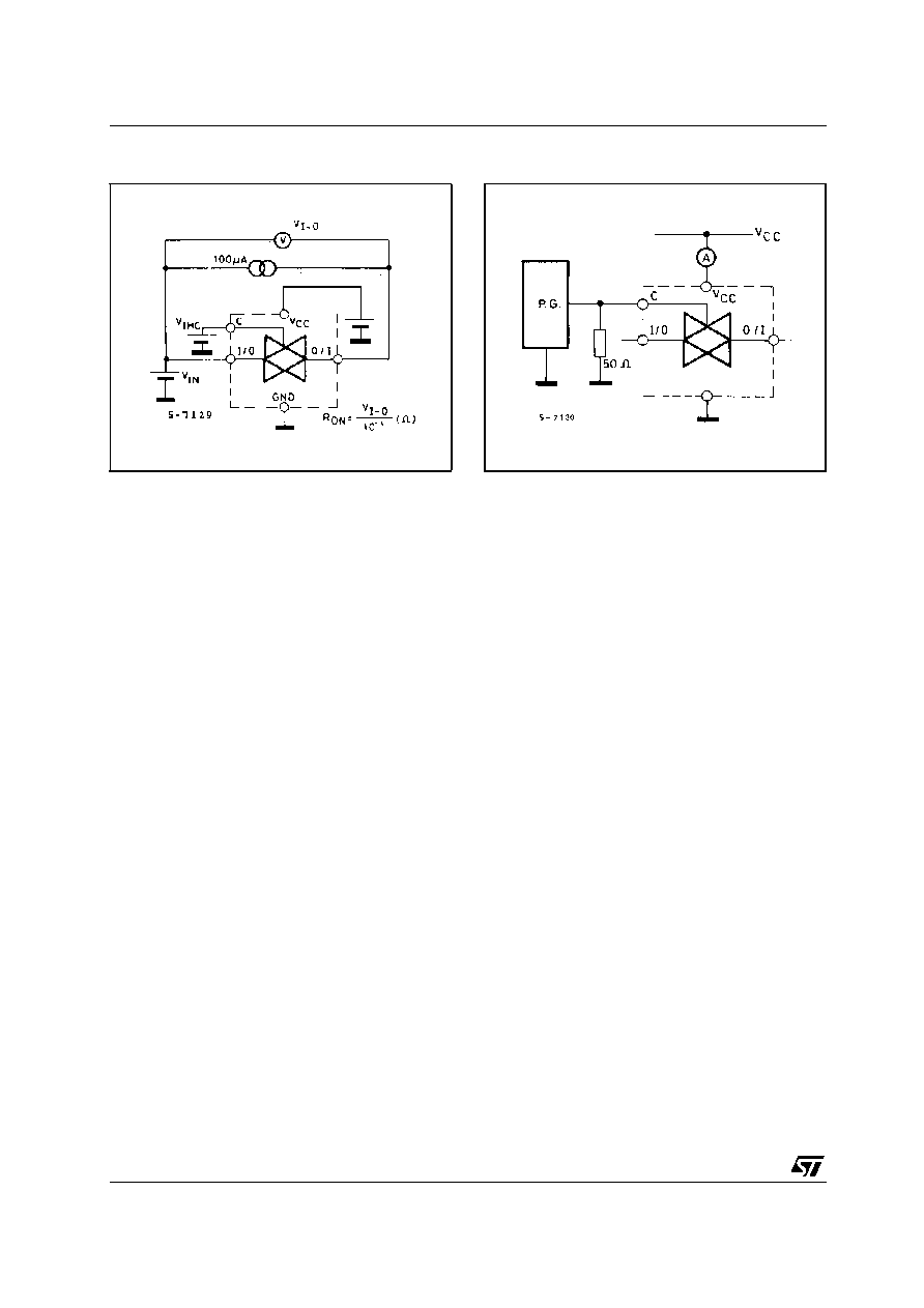
SWITCHING CARACTERISTICS TEST CIRCUIT
CROSSTALK (control to output)
BANDWIDTH AND FEEDTHROUGH ATTENUATION
MAXIMUM CONTROL FREQUENCY
74LVQ4066
6/11
CHANNEL RESISTANCE (R
ON)
I
CC
(Opr.)
74LVQ4066
7/11
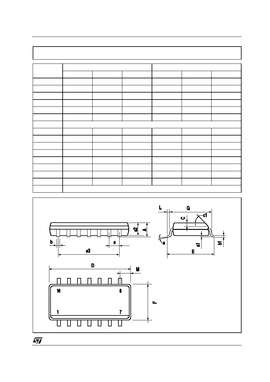
DIM.
mm.
inch
MIN.
TYP
MAX.
MIN.
TYP.
MAX.
A
1.75
0.068
a1
0.1
0.2
0.003
0.007
a2
1.65
0.064
b
0.35
0.46
0.013
0.018
b1
0.19
0.25
0.007
0.010
C
0.5
0.019
c1
45∞ (typ.)
D
8.55
8.75
0.336
0.344
E
5.8
6.2
0.228
0.244
e
1.27
0.050
e3
7.62
0.300
F
3.8
4.0
0.149
0.157
G
4.6
5.3
0.181
0.208
L
0.5
1.27
0.019
0.050
M
0.68
0.026
S
∞ (max.)
SO-14 MECHANICAL DATA
PO13G
8
74LVQ4066
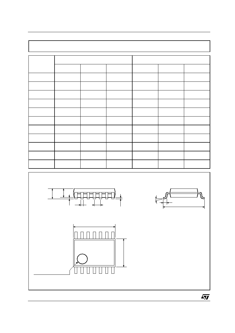
8/11
DIM.
mm.
inch
MIN.
TYP
MAX.
MIN.
TYP.
MAX.
A
1.2
0.047
A1
0.05
0.15
0.002
0.004
0.006
A2
0.8
1
1.05
0.031
0.039
0.041
b
0.19
0.30
0.007
0.012
c
0.09
0.20
0.004
0.0089
D
4.9
5
5.1
0.193
0.197
0.201
E
6.2
6.4
6.6
0.244
0.252
0.260
E1
4.3
4.4
4.48
0.169
0.173
0.176
e
0.65 BSC
0.0256 BSC
K
0∞
8∞
0∞
8∞
L
0.45
0.60
0.75
0.018
0.024
0.030
TSSOP14 MECHANICAL DATA
c
E
b
A2
A
E1
D
1
PIN 1 IDENTIFICATION
A1
L
K
e
0080337D

74LVQ4066
9/11
DIM.
mm.
inch
MIN.
TYP
MAX.
MIN.
TYP.
MAX.
A
330
12.992
C
12.8
13.2
0.504
0.519
D
20.2
0.795
N
60
2.362
T
22.4
0.882
Ao
6.4
6.6
0.252
0.260
Bo
9
9.2
0.354
0.362
Ko
2.1
2.3
0.082
0.090
Po
3.9
4.1
0.153
0.161
P
7.9
8.1
0.311
0.319
Tape & Reel SO-14 MECHANICAL DATA

74LVQ4066
10/11
DIM.
mm.
inch
MIN.
TYP
MAX.
MIN.
TYP.
MAX.
A
330
12.992
C
12.8
13.2
0.504
0.519
D
20.2
0.795
N
60
2.362
T
22.4
0.882
Ao
6.7
6.9
0.264
0.272
Bo
5.3
5.5
0.209
0.217
Ko
1.6
1.8
0.063
0.071
Po
3.9
4.1
0.153
0.161
P
7.9
8.1
0.311
0.319
Tape & Reel TSSOP14 MECHANICAL DATA

74LVQ4066
11/11
Information furnished is believed to be accurate and reliable. However, STMicroelectronics assumes no responsibility for the
consequences of use of such information nor for any infringement of patents or other rights of third parties which may result from
its use. No license is granted by implication or otherwise under any patent or patent rights of STMicroelectronics. Specifications
mentioned in this publication are subject to change without notice. This publication supersedes and replaces all information
previously supplied. STMicroelectronics products are not authorized for use as critical components in life support devices or
systems without express written approval of STMicroelectronics.
© The ST logo is a registered trademark of STMicroelectronics
© 2003 STMicroelectronics - Printed in Italy - All Rights Reserved
STMicroelectronics GROUP OF COMPANIES
Australia - Brazil - Canada - China - Finland - France - Germany - Hong Kong - India - Israel - Italy - Japan - Malaysia - Malta - Morocco
Singapore - Spain - Sweden - Switzerland - United Kingdom - United States.
© http://www.st.com