 | ÐлекÑÑоннÑй компоненÑ: 74LVX27T | СкаÑаÑÑ:  PDF PDF  ZIP ZIP |
LOW VOLTAGE TRIPLE 3-INPUT NOR GATE
1/8
July 2001
s
HIGH SPEED :
t
PD
= 4.1ns (TYP.) at V
CC
= 3.3V
s
5V TOLERANT INPUTS
s
INPUT VOLTAGE LEVEL :
V
IL
=0.8V, V
IH
=2V at V
CC
=3V
s
LOW POWER DISSIPATION:
I
CC
= 2
µ
A (MAX.) at T
A
=25°C
s
LOW NOISE:
V
OLP
= 0.3V (TYP.) at V
CC
= 3.3V
s
SYMMETRICAL OUTPUT IMPEDANCE:
|I
OH
| = I
OL
= 4mA (MIN)
s
BALANCED PROPAGATION DELAYS:
t
PLH
t
PHL
s
OPERATING VOLTAGE RANGE:
V
CC
(OPR) = 2V to 3.6V (1.2V Data Retention)
s
PIN AND FUNCTION COMPATIBLE WITH
74 SERIES 27
s
IMPROVED LATCH-UP IMMUNITY
s
POWER DOWN PROTECTION ON INPUTS
DESCRIPTION
The 74LVX27 is a low voltage CMOS TRIPLE
3-INPUT NOR GATE fabricated with sub-micron
silicon gate and double-layer metal wiring C
2
MOS
technology. It is ideal for low power, battery
operated and low noise 3.3V applications.
The internal circuit is composed of 3 stages
including buffer output, which provides high noise
immunity and stable output.
Power down protection is provided on all inputs
and 0 to 7V can be accepted on inputs with no
regard to the supply voltage.
This device can be used to interface 5V to 3V
system. It combines high speed performance with
the true CMOS low power consumption.
All inputs and outputs are equipped with
protection circuits against static discharge, giving
them 2KV ESD immunity and transient excess
voltage.
74LVX27
LOW VOLTAGE CMOS TRIPLE 3-INPUT NOR GATE
WITH 5V TOLERANT INPUTS
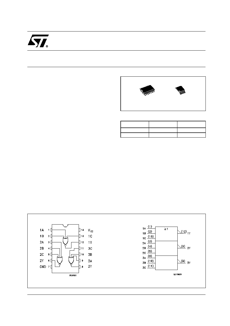
PIN CONNECTION AND IEC LOGIC SYMBOLS
ORDER CODES
PACKAGE
TUBE
T & R
SOP
74LVX27M
74LVX27MTR
TSSOP
74LVX27TTR
TSSOP
SOP
74LVX27
2/8
INPUT EQUIVALENT CIRCUIT
PIN DESCRIPTION
TRUTH TABLE
X : Don`t Care
ABSOLUTE MAXIMUM RATINGS
Absolute Maximum Ratings are those values beyond which damage to the device may occur. Functional operation under these conditions is
not implied.
RECOMMENDED OPERATING CONDITIONS
1) Truth Table guaranteed: 1.2V to 3.6V
2) V
IN
from 0.8V to 2.0V
PIN No
SYMBOL
NAME AND FUNCTION
1, 3, 9
1A to 3A
Data Inputs
2, 4, 10
1B to 3B
Data Inputs
13, 5, 11
1C to 3C
Data Inputs
12, 6, 8
1Y to 3Y
Data Outputs
7
GND
Ground (0V)
14
V
CC
Positive Supply Voltage
A
B
C
Y
L
L
L
H
H
X
X
L
X
H
X
L
X
X
H
L
Symbol
Parameter
Value
Unit
V
CC
Supply Voltage
-0.5 to +7.0
V
V
I
DC Input Voltage
-0.5 to +7.0
V
V
O
DC Output Voltage
-0.5 to V
CC
+ 0.5
V
I
IK
DC Input Diode Current
- 20
mA
I
OK
DC Output Diode Current
±
20
mA
I
O
DC Output Current
±
25
mA
I
CC
or I
GND
DC V
CC
or Ground Current
±
50
mA
T
stg
Storage Temperature
-65 to +150
°C
T
L
Lead Temperature (10 sec)
300
°C
Symbol
Parameter
Value
Unit
V
CC
Supply Voltage (note 1)
2 to 3.6
V
V
I
Input Voltage
0 to 5.5
V
V
O
Output Voltage
0 to V
CC
V
T
op
Operating Temperature
-55 to 125
°C
dt/dv
Input Rise and Fall Time (note 2) (V
CC
= 3.3V)
0 to 100
ns/V
74LVX27
3/8
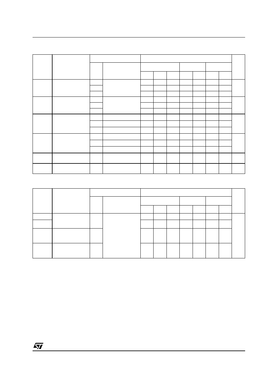
DC SPECIFICATIONS
DYNAMIC SWITCHING CHARACTERISTICS
1) Worst case package.
2) Max number of outputs defined as (n). Data inputs are driven 0V to 3.3V, (n-1) outputs switching and one output at GND.
3) Max number of data inputs (n) switching. (n-1) switching 0V to 3.3V. Inputs under test switching: 3.3V to threshold (V
ILD
), 0V to threshold
(V
IHD
), f=1MHz.
Symbol
Parameter
Test Condition
Value
Unit
V
CC
(V)
T
A
= 25°C
-40 to 85°C
-55 to 125°C
Min.
Typ.
Max.
Min.
Max.
Min.
Max.
V
IH
High Level Input
Voltage
2.0
1.5
1.5
1.5
V
3.0
2.0
2.0
2.0
3.6
2.4
2.4
2.4
V
IL
Low Level Input
Voltage
2.0
0.5
0.5
0.5
V
3.0
0.8
0.8
0.8
3.6
0.8
0.8
0.8
V
OH
High Level Output
Voltage
2.0
I
O
=-50
µ
A
1.9
2.0
1.9
1.9
V
3.0
I
O
=-50
µ
A
2.9
3.0
2.9
2.9
3.0
I
O
=-4 mA
2.58
2.48
2.4
V
OL
Low Level Output
Voltage
2.0
I
O
=50
µ
A
0.0
0.1
0.1
0.1
V
3.0
I
O
=50
µ
A
0.0
0.1
0.1
0.1
3.0
I
O
=4 mA
0.36
0.44
0.55
I
I
Input Leakage
Current
3.6
V
I
= 5V or GND
±
0.1
±
1
±
1
µ
A
I
CC
Quiescent Supply
Current
3.6
V
I
= V
CC
or GND
2
20
20
µ
A
Symbol
Parameter
Test Condition
Value
Unit
V
CC
(V)
T
A
= 25°C
-40 to 85°C
-55 to 125°C
Min.
Typ.
Max.
Min.
Max.
Min.
Max.
V
OLP
Dynamic Low
Voltage Quiet
Output (note 1, 2)
3.3
C
L
= 50 pF
0.3
0.5
V
V
OLV
-0.5
-0.3
V
IHD
Dynamic High
Voltage Input (note
1, 3)
3.3
2
V
ILD
Dynamic Low
Voltage Input (note
1, 3)
3.3
0.8
74LVX27
4/8
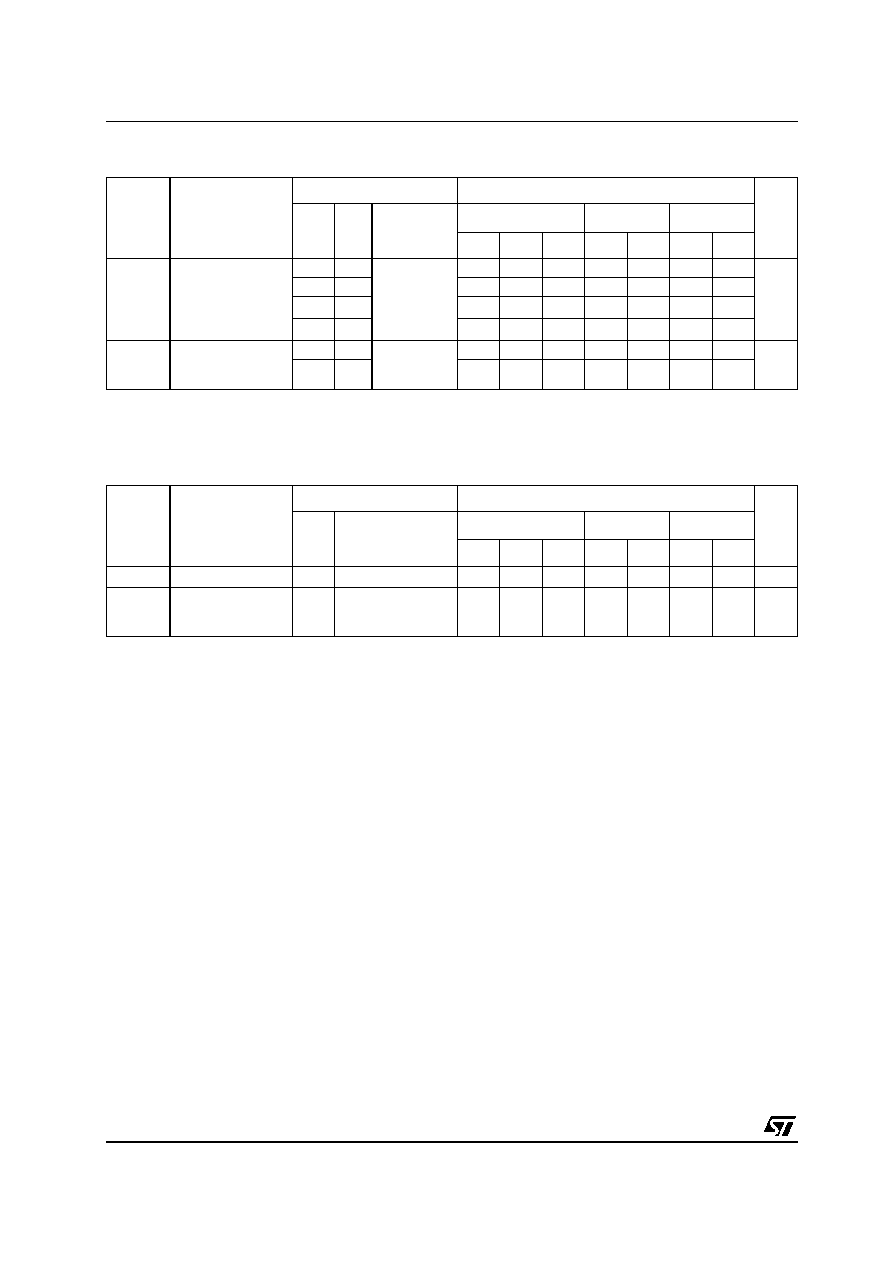
AC ELECTRICAL CHARACTERISTICS (Input t
r
= t
f
= 3ns)
1) Skew is defined as the absolute value of the difference between the actual propagation delay for any two outputs of the same device switch-
ing in the same direction, either HIGH or LOW
2) Parameter guaranteed by design
(*) Voltage range is 3.3V
±
0.3V
CAPACITIVE CHARACTERISTICS
1) C
PD
is defined as the value of the IC's internal equivalent capacitance which is calculated from the operating current consumption without
load. (Refer to Test Circuit). Average operating current can be obtained by the following equation. I
CC(opr)
= C
PD
x V
CC
x f
IN
+ I
CC
/3 (per gate)
Symbol
Parameter
Test Condition
Value
Unit
V
CC
(V)
C
L
(pF)
T
A
= 25°C
-40 to 85°C
-55 to 125°C
Min.
Typ.
Max.
Min.
Max.
Min.
Max.
t
PLH
t
PHL
Propagation Delay
Time
2.7
15
5.2
8.6
1.0
10.5
1.0
12.0
ns
2.7
50
8.0
13.5
1.0
15.4
1.0
17.0
3.3
(*)
15
4.1
6.2
1.0
7.5
1.0
9.0
3.3
(*)
50
6.6
9.7
1.0
11.0
1.0
12.5
t
OSLH
t
OSHL
Output To Output
Skew Time (note1,
2)
2.7
50
0.5
1.0
1.5
1.5
ns
3.3
(*)
50
0.5
1.0
1.5
1.5
Symbol
Parameter
Test Condition
Value
Unit
V
CC
(V)
T
A
= 25°C
-40 to 85°C
-55 to 125°C
Min.
Typ.
Max.
Min.
Max.
Min.
Max.
C
IN
Input Capacitance
3.3
4
10
10
10
pF
C
PD
Power Dissipation
Capacitance
(note 1)
3.3
19
pF
74LVX27
5/8
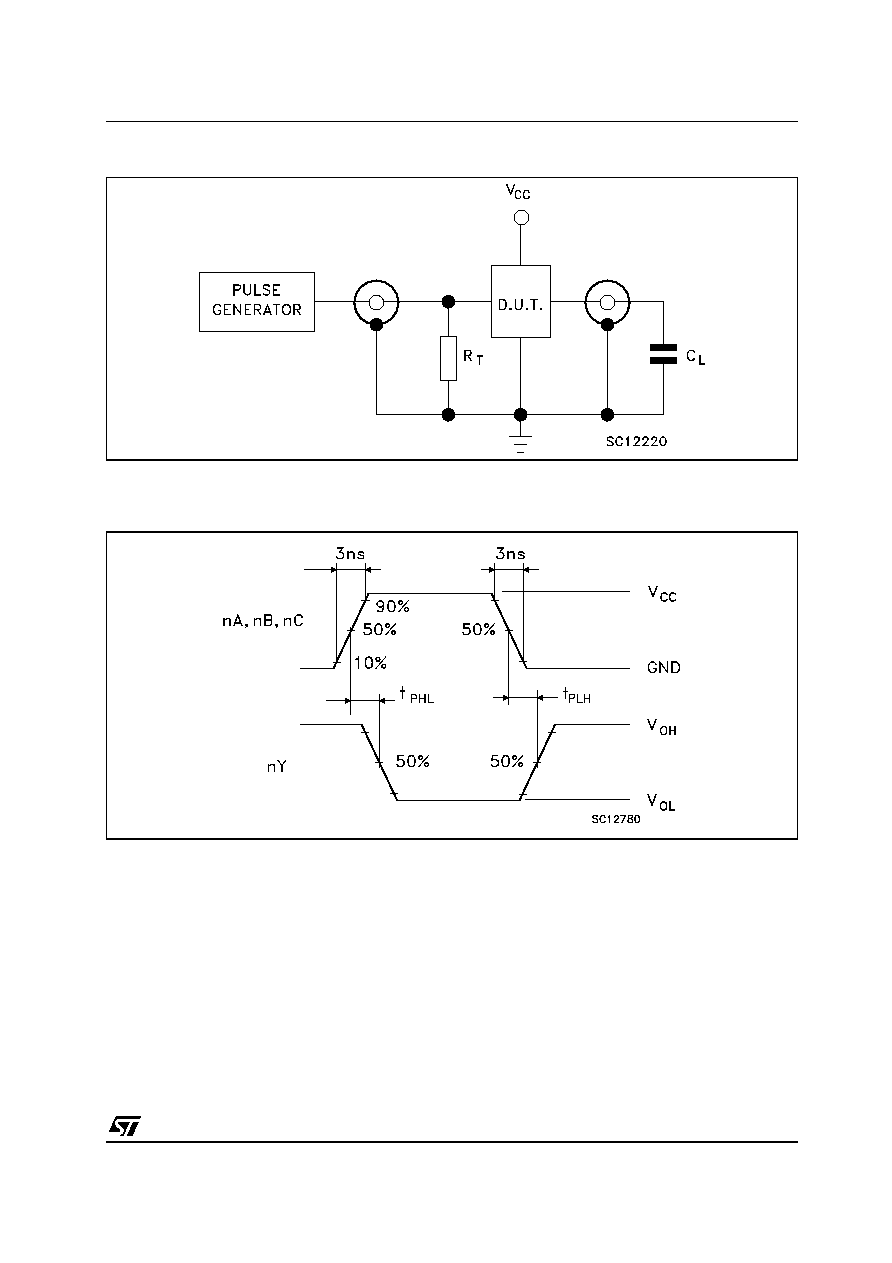
TEST CIRCUIT
C
L
=15/50pF or equivalent (includes jig and probe capacitance)
R
T
= Z
OUT
of pulse generator (typically 50
)
WAVEFORM: PROPAGATION DELAYS (f=1MHz; 50% duty cycle)
74LVX27
6/8
DIM.
mm.
inch
MIN.
TYP
MAX.
MIN.
TYP.
MAX.
A
1.75
0.068
a1
0.1
0.2
0.003
0.007
a2
1.65
0.064
b
0.35
0.46
0.013
0.018
b1
0.19
0.25
0.007
0.010
C
0.5
0.019
c1
45° (typ.)
D
8.55
8.75
0.336
0.344
E
5.8
6.2
0.228
0.244
e
1.27
0.050
e3
7.62
0.300
F
3.8
4.0
0.149
0.157
G
4.6
5.3
0.181
0.208
L
0.5
1.27
0.019
0.050
M
0.68
0.026
S
8° (max.)
SO-14 MECHANICAL DATA
PO13G
74LVX27
7/8
DIM.
mm.
inch
MIN.
TYP
MAX.
MIN.
TYP.
MAX.
A
1.2
0.047
A1
0.05
0.15
0.002
0.004
0.006
A2
0.8
1
1.05
0.031
0.039
0.041
b
0.19
0.30
0.007
0.012
c
0.09
0.20
0.004
0.0089
D
4.9
5
5.1
0.193
0.197
0.201
E
6.2
6.4
6.6
0.244
0.252
0.260
E1
4.3
4.4
4.48
0.169
0.173
0.176
e
0.65 BSC
0.0256 BSC
K
0°
8°
0°
8°
L
0.45
0.60
0.75
0.018
0.024
0.030
TSSOP14 MECHANICAL DATA
c
E
b
A2
A
E1
D
1
PIN 1 IDENTIFICATION
A1
L
K
e
0080337D

74LVX27
8/8
Information furnished is believed to be accurate and reliable. However, STMicroelectronics assumes no responsibility for the
consequences of use of such information nor for any infringement of patents or other rights of third parties which may result from
its use. No license is granted by implication or otherwise under any patent or patent rights of STMicroelectronics. Specifications
mentioned in this publication are subject to change without notice. This publication supersedes and replaces all information
previously supplied. STMicroelectronics products are not authorized for use as critical components in life support devices or
systems without express written approval of STMicroelectronics.
© The ST logo is a registered trademark of STMicroelectronics
© 2001 STMicroelectronics - Printed in Italy - All Rights Reserved
STMicroelectronics GROUP OF COMPANIES
Australia - Brazil - China - Finland - France - Germany - Hong Kong - India - Italy - Japan - Malaysia - Malta - Morocco
Singapore - Spain - Sweden - Switzerland - United Kingdom
© http://www.st.com