1/9
November 2001
s
HIGH SPEED: t
PD
=3.7ns (TYP.) at V
CC
= 5V
s
LOW POWER DISSIPATION:
I
CC
= 1
µ
A(MAX.) at T
A
=25∞C
s
HIGH NOISE IMMUNITY:
V
NIH
= V
NIL
= 28% V
CC
(MIN.)
s
POWER DOWN PROTECTION ON INPUT
s
OPERATING VOLTAGE RANGE:
V
CC
(OPR) = 2V to 5.5V
s
IMPROVED LATCH-UP IMMUNITY
DESCRIPTION
The 74V2G07 is an advanced high-speed CMOS
TRIPLE BUFFER (OPEN DRAIN) fabricated with
sub-micron silicon gate and double-layer metal
wiring C
2
MOS technology.
The internal circuit is composed of 2 stages
including buffer output, which provide high noise
immunity and stable output.
Power down protection is provided on input and 0
to 7V can be accepted on input with no regard to
the supply voltage. This device can be used to
interface 5V to 3V.
74V2G07
TRIPLE BUFFER (OPEN DRAIN)
This is preliminary information on a new product now in development are or undergoing evaluation. Details subject to change without notice.
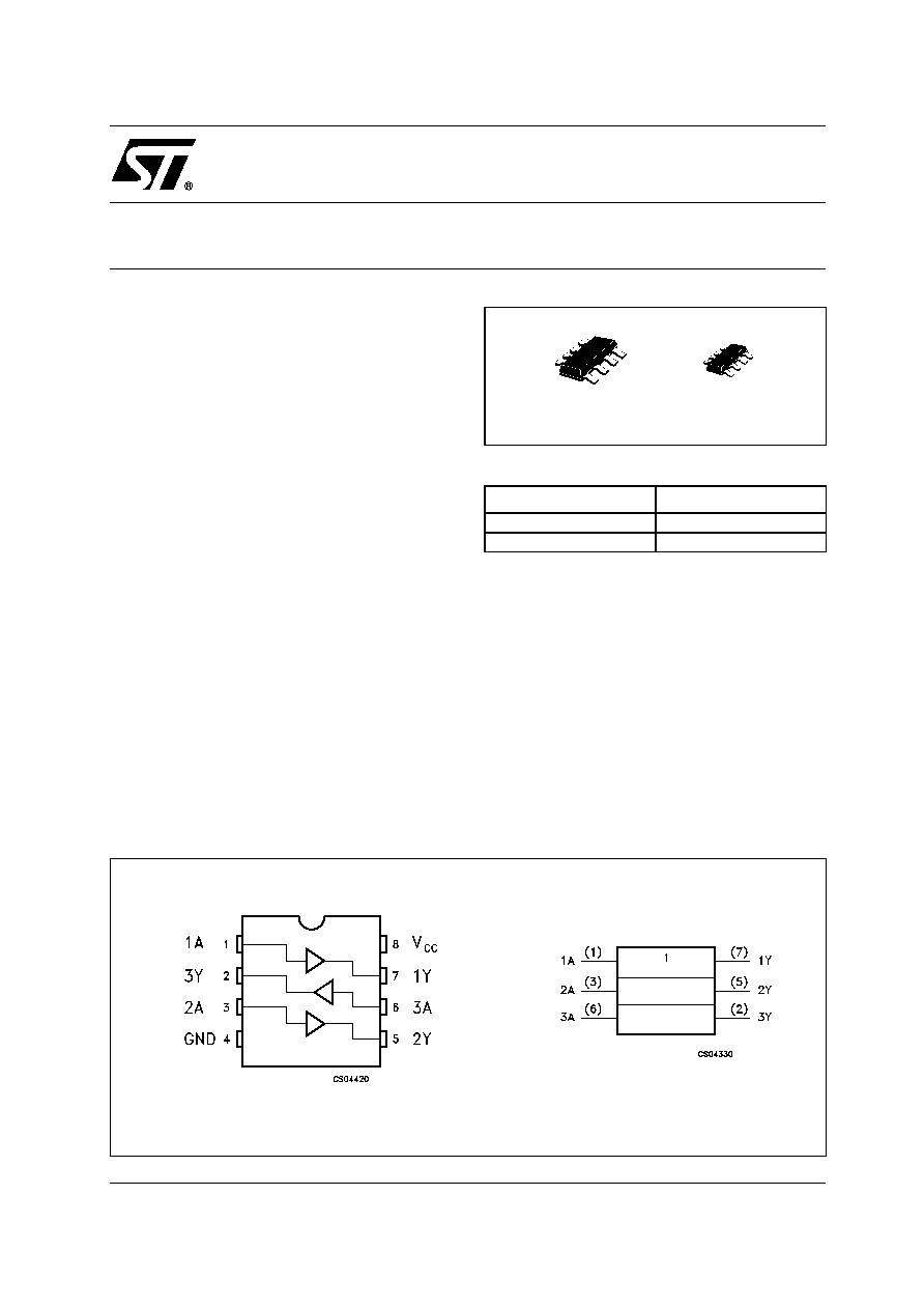
PIN CONNECTION AND IEC LOGIC SYMBOLS
ORDER CODES
PACKAGE
T & R
SOT23-8L
74V2G07STR
SOT323-8L
74V2G07CTR
SOT323-8L
SOT23-8L
PRELIMINARY DATA
74V2G07
2/9
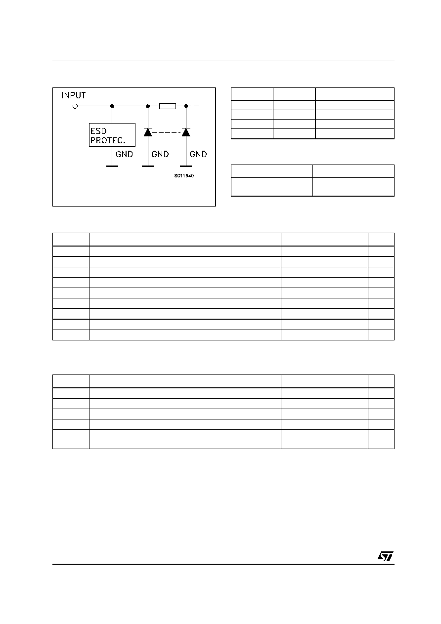
INPUT EQUIVALENT CIRCUIT
PIN DESCRIPTION
TRUTH TABLE
Z: High Impedance
ABSOLUTE MAXIMUM RATINGS
Absolute Maximum Ratings are those values beyond which damage to the device may occur. Functional operation under these conditions is
not implied.
RECOMMENDED OPERATING CONDITIONS
1) V
IN
from 30% to 70% of V
CC
PIN No
SYMBOL
NAME QND FUNCTION
1, 3, 6
1A, 2A, 3A
Data Inputs
7, 5, 2
1Y, 2Y, 3Y
Data Outputs
4
GND
Ground (0V)
8
V
CC
Positive Supply Voltage
A
Y
L
L
H
Z
Symbol
Parameter
Value
Unit
V
CC
Supply Voltage
-0.5 to +7.0
V
V
I
DC Input Voltage
-0.5 to +7.0
V
V
O
DC Output Voltage
-0.5 to V
CC
+ 0.5
V
I
IK
DC Input Diode Current
- 20
mA
I
OK
DC Output Diode Current
±
20
mA
I
O
DC Output Current
±
25
mA
I
CC
or I
GND
DC V
CC
or Ground Current
±
50
mA
T
stg
Storage Temperature
-65 to +150
∞C
T
L
Lead Temperature (10 sec)
260
∞C
Symbol
Parameter
Value
Unit
V
CC
Supply Voltage
2 to 5.5
V
V
I
Input Voltage
0 to 5.5
V
V
O
Output Voltage
0 to V
CC
V
T
op
Operating Temperature
-55 to 125
∞C
dt/dv
Input Rise and Fall Time (note 1) (V
CC
= 3.3
±
0.3V)
(V
CC
= 5.0
±
0.5V)
0 to 100
0 to 20
ns/V
ns/V
74V2G07
3/9
DC SPECIFICATIONS
AC ELECTRICAL CHARACTERISTICS (Input t
r
= t
f
= 3ns)
(*) Voltage range is 3.3V
±
0.3V
(**) Voltage range is 5.0V
±
0.5V
Symbol
Parameter
Test Condition
Value
Unit
V
CC
(V)
T
A
= 25∞C
-40 to 85∞C
-55 to 125∞C
Min.
Typ.
Max.
Min.
Max.
Min.
Max.
V
IH
High Level Input
Voltage
2.0
1.5
1.5
1.5
V
3.0 to
5.5
0.7V
CC
0.7V
CC
0.7V
CC
V
IL
Low Level Input
Voltage
2.0
0.5
0.5
0.5
V
3.0 to
5.5
0.3V
CC
0.3V
CC
0.3V
CC
V
OL
Low Level Output
Voltage
2.0
I
O
=50
µ
A
0.0
0.1
0.1
0.1
V
3.0
I
O
=50
µ
A
0.0
0.1
0.1
0.1
4.5
I
O
=50
µ
A
0.0
0.1
0.1
0.1
3.0
I
O
=4 mA
0.36
0.44
0.55
4.5
I
O
=8 mA
0.36
0.44
0.55
I
OZ
High Impedance
Output Leakage
Current
5.5
V
I
= V
IH
or V
IL
V
O
= V
CC
or GND
±
0.25
±
2.5
±
5
µ
A
I
I
Input Leakage
Current
0 to
5.5
V
I
= 5.5V or GND
±
0.1
±
1
±
1
µ
A
I
CC
Quiescent Supply
Current
5.5
V
I
= V
CC
or GND
1
10
20
µ
A
Symbol
Parameter
Test Condition
Value
Unit
V
CC
(V)
C
L
(pF)
T
A
= 25∞C
-40 to 85∞C
-55 to 125∞C
Min.
Typ.
Max.
Min.
Max.
Min.
Max.
t
PZL
Propagation Delay
Time
3.3
(*)
15
4.8
7.7
1.0
9.0
1.0
10.0
ns
3.3
(*)
50
5.3
8.5
1.0
10.0
1.0
11.0
5.0
(**)
15
3.7
5.5
1.0
6.5
1.0
7.5
5.0
(**)
50
4.2
7.5
1.0
8.5
1.0
9.5
t
PLZ
Propagation Delay
Time
3.3
(*)
50
7.5
10.5
1.0
11.5
1.0
12.5
ns
5.0
(**)
50
4.7
7.5
1.0
8.5
1.0
9.5
74V2G07
4/9
CAPACITIVE CHARACTERISTICS
1) C
PD
is defined as the value of the IC's internal equivalent capacitance which is calculated from the operating current consumption without
load. (Refer to Test Circuit). Average operating current can be obtained by the following equation. I
CC(opr)
= C
PD
x V
CC
x f
IN
+ I
CC
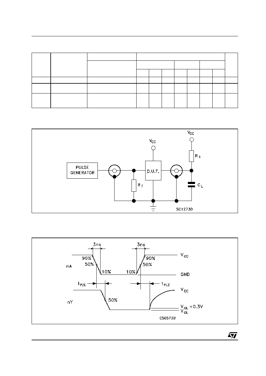
TEST CIRCUIT
C
L
= 15/50pF or equivalent (includes jig and probe capacitance)
R
1
= 1K
or equivalent
R
T
= Z
OUT
of pulse generator (typically 50
)
WAVEFORM: PROPAGATION DELAY (f=1MHz; 50% duty cycle)
Symbol
Parameter
Test Condition
Value
Unit
T
A
= 25∞C
-40 to 85∞C
-55 to 125∞C
Min.
Typ.
Max.
Min.
Max.
Min.
Max.
C
IN
Input Capacitance
4
10
10
10
pF
C
OUT
Output
Capacitance
5
10
10
10
pF
C
PD
Power Dissipation
Capacitance
(note 1)
3
pF

74V2G07
5/9
DIM.
mm.
mils
MIN.
TYP
MAX.
MIN.
TYP.
MAX.
A
0.90
1.45
35.4
57.1
A1
0.00
0.15
0.0
5.9
A2
0.90
1.30
35.4
51.2
b
0.22
0.38
8.6
14.9
C
0.09
0.20
3.5
7.8
D
2.80
3.00
110.2
118.1
E
2.60
3.00
102.3
118.1
E1
1.50
1.75
59.0
68.8
e
0
.65
25.6
e1
1.95
76.7
L
0.35
0.55
13.7
21.6
SOT23-8L MECHANICAL DATA