1/9
June 2003
s
HIGH SPEED:
t
PD
= 0.6ns (TYP.) at V
CC
= 5V
s
COMPATIBLE WITH TTL LEVEL
s
LOW POWER DISSIPATION:
I
CC
= 1
µ
A(MAX.) at T
A
= 25∞C
s
LOW "ON" RESISTANCE:
R
ON
=10
(TYP.) AT V
CC
= 5V I
I/O
= 1mA
s
SINE WAVE DISTORTION:
0.04% AT V
CC
= 5.0V, f = 1KHz
s
OPERATING VOLTAGE RANGE:
V
CC
(OPR) = 4.5V TO 5.5V
s
IMPROVED LATCH-UP IMMUNITY
DESCRIPTION
The 74V2T66 is an advanced high-speed CMOS
DUAL BILATERAL SWITCH fabricated in silicon
gate C
2
MOS technology. It achieves high speed
propagation
delay
and
VERY
LOW
ON
resistances while maintaining true CMOS low
power consumption. This bilateral switch handles
rail to rail analog and digital signals that may vary
across the full power supply range (from GND to
V
CC
)
The C input is provided to control the switch and
it's compatible with standard CMOS output; the
switch is ON (port I/O is connected to Port O/I)
when the C input is held high and OFF (high
impedance state exists between the two ports)
when C is held low. It can be used in many
application as Battery Powered System, Test
Equipment. It's available in the commercial and
extended
temperature
range
in
SOT23-8L
package. All inputs and output are equipped with
protection circuits against static discharge, giving
them ESD immunity and transient excess voltage.
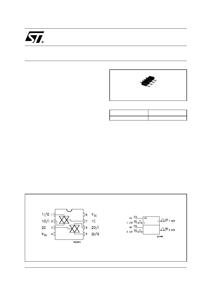
74V2T66
DUAL BILATERAL SWITCH
PIN CONNECTION AND IEC LOGIC SYMBOLS
ORDER CODES
PACKAGE
T & R
SOT23-8L
74V2T66STR
SOT23-8L

74V2T66
2/9
INPUT EQUIVALENT CIRCUIT
PIN DESCRIPTION
TRUTH TABLE
* : High Impedance State
ABSOLUTE MAXIMUM RATINGS
Absolute Maximum Ratings are those values beyond which damage to the device may occur. Functional operation under these conditions is
not implied
RECOMMENDED OPERATING CONDITIONS
1) V
IN
from 0.8V to 2V on control pin
PIN No
SYMBOL
NAME AND FUNCTION
1, 5
1I/O, 2I/O
Independent Input/Output
2, 6
1O/I, 2O/I
Independent Output/Input
7, 3
1C, 2C
Enable Input (Active
HIGH)
4
GND
Ground (0V)
8
V
CC
Positive Supply Voltage
CONTROL
SWITCH FUNCTION
H
ON
L
OFF *
Symbol
Parameter
Value
Unit
V
CC
Supply Voltage
-0.5 to +7.0
V
V
I
DC Input Voltage
-0.5 to V
CC
+ 0.5
V
V
IC
DC Control Input Voltage
-0.5 to +7.0
V
V
O
DC Output Voltage
-0.5 to V
CC
+ 0.5
V
I
IK
DC Input Diode Current
±
20
mA
I
IK
DC Control Input Diode Current
- 20
mA
I
OK
DC Output Diode Current
±
20
mA
I
O
DC Output Current
±
50
mA
I
CC
or I
GND
DC V
CC
or Ground Current
±
50
mA
T
stg
Storage Temperature
-65 to +150
∞C
T
L
Lead Temperature (10 sec)
300
∞C
Symbol
Parameter
Value
Unit
V
CC
Supply Voltage
4.5 to 5.5
V
V
I
Input Voltage
0 to V
CC
V
V
IC
Control Input Voltage
0 to 5.5
V
V
O
Output Voltage
0 to V
CC
V
T
op
Operating Temperature
-55 to 125
∞C
dt/dv
Input Rise and Fall Time (note 1) V
CC
= 5.0V
0 to 20
ns/V
74V2T66
3/9
DC SPECIFICATIONS
(*) Voltage range is 5V
±
0.5V
AC ELECTRICAL CHARACTERISTICS (C
L
= 50pF, Input t
r
= t
f
= 3ns)
(*) Voltage range is 5.0V
±
0.5V
Symbol
Parameter
Test Condition
Value
Unit
V
CC
(V)
T
A
= 25∞C
-40 to 85∞C
-55 to 125∞C
Min.
Typ.
Max.
Min.
Max.
Min.
Max.
V
IH
High Level Input
Voltage
5.0
(*)
2
2
2
V
V
IL
Low Level Input
Voltage
5.0
(*)
0.8
0.8
0.8
V
R
ON
ON Resistance
5.0
(*)
V
IC
= V
IH
V
I/O
= V
CC
to GND
I
I/O
1mA
12
17
20
24
V
R
ON
ON Resistance
5.0
(*)
V
IC
= V
IH
V
I/O
= V
CC
or GND
I
I/O
1mA
10
14
18
20
V
I
OFF
Input/Output
Leakage Current
(SWITCH OFF)
5.5
V
OS
= V
CC
to GND
V
IS
= V
CC
to GND
V
IC
= V
IL
±
0.1
±
1
±
1
µ
A
I
IZ
Switch Input
Leakage Current
(SWITCH ON,
OUTPUT OPEN)
5.5
V
OS
= V
CC
to GND
V
IC
= V
IH
±
0.1
±
1
±
5
µ
A
I
IN
Control Input
Leakage Current
0 to
5.5
V
IC
= 5.5V or GND
±
0.1
±
1.0
±
1.0
µ
A
I
CC
Quiescent Supply
Current
5.5
V
I
= V
CC
or GND
1
10
20
µ
A
Symbol
Parameter
Test Condition
Value
Unit
V
CC
(V)
T
A
= 25∞C
-40 to 85∞C
-55 to 125∞C
Min.
Typ.
Max.
Min.
Max.
Min.
Max.
t
PD
Delay Time
5.0
(*)
0.6
0.7
1.0
2.0
ns
t
PLZ
t
PHZ
Output Disable
Time
5.0
(*)
R
L
= 500
6.0
7.5
9.0
10.0
ns
t
PZL
t
PZH
Output Enable
Time
5.0
(*)
R
L
= 1 K
2.5
4.0
5.0
7.0
ns

74V2T66
4/9
CAPACITIVE CHARACTERISTICS
1) C
PD
is defined as the value of the IC's internal equivalent capacitance which is calculated from the operating current consumption without
load. (Refer to Test Circuit). Average operating current can be obtained by the following equation. I
CC(opr)
= C
PD
x V
CC
x f
IN
+ I
CC
/2(per switch)
ANALOG SWITCH CHARACTERISTICS (GND = 0V; T
A
= 25∞C)
(*) Voltage range is 5.0V
±
0.5V
Symbol
Parameter
Test Condition
Value
Unit
T
A
= 25∞C
-40 to 85∞C
-55 to 125∞C
Min.
Typ.
Max.
Min.
Max.
Min.
Max.
C
IN
Input Capacitance
4
10
10
10
pF
C
I/O
Output
Capacitance
10
pF
C
PD
Power Dissipation
Capacitance
(note 1)
3
pF
Symbol
Parameter
Test Condition
Value
Unit
V
CC
(V)
V
IN
(V
p-p
)
Typ.
Sine Wave
Distortion (THD)
5.0(*)
4
f
IN
= 1 KHz R
L
= 10 K
, C
L
= 50 pF
0.04
%
f
MAX
Frequency
Response
(Switch ON)
5.0(*)
Adjust f
IN
voltage to obtain 0 dBm at V
OS
.
Increase f
IN
Frequency until dB meter reads -3dB
R
L
= 50
, C
L
= 10 pF
180
MHz
Feedthrough
Attenuation
(Switch OFF)
5.0(*)
V
IN
is centered at V
CC
/2
Adjust f
IN
Voltage to obtained 0dBm at V
IS
R
L
= 600
, C
L
= 50 pF, f
IN
= 1MHz sine wave
-60
dB
Crosstalk (Control
Input to Signal
Output)
5.0(*)
R
L
= 600
, C
L
= 50 pF, f
IN
= 1MHz square wave
tr=tf= 2.0ns
60
mV
Crosstalk Between
Switches
5.0(*)
R
L
= 600
, C
L
= 50 pF, f
IN
= 1MHz sine wave
-60
dB
74V2T66
5/9
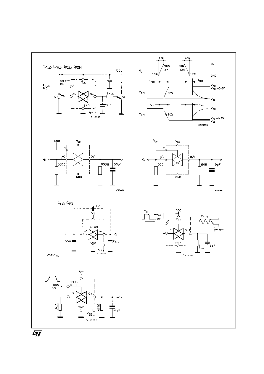
SWITCHING CARACTERISTICS TEST CIRCUIT
FEEDTHROUGH ATTENUATION
CROSSTALK (control to output
BANDWIDTH ATTENUATION
MAXIMUM CONTROL FREQUENCY