
1/17
June 2004
s
HIGH SPEED: t
PD
= 4.4ns (MAX.) at T
A
=85∞C
V
CCA
= 3.0V V
CCB
= 2.3V
s
LOW POWER DISSIPATION:
I
CCA
= I
CCB
= 20
µ
A(MAX.) at T
A
=85∞C
s
SYMMETRICAL OUTPUT IMPEDANCE:
|I
OHA
| = I
OLA
= 8mA MIN at
V
CCA
= 3.0V; V
CCB
= 1.65V or 2.3V
|I
OHB
| = I
OLB
= 6mA (MIN at
V
CCA
= 2.3V or 3.0V; V
CCB
= 1.65V)
s
BALANCED PROPAGATION DELAYS:
t
PLH
t
PHL
s
POWER DOWN PROTECTION ON INPUTS
AND OUTPUTS
s
SERIES RESISTOR ON A SIDE
s
OPERATING VOLTAGE RANGE:
V
CCA
(OPR) = 2.3V to 3.6V (1.2V Data
Retention)
V
CCB
(OPR) = 1.65V to2.7V (1.2V Data
Retention)
s
PIN AND FUNCTION COMPATIBLE WITH
74 SERIES 16245
s
BUS HOLD PROVIDED ON DATA INPUT
BOTH SIDE
s
LATCH-UP PERFORMANCE EXCEEDS
500mA (JESD 17)
s
ESD PERFORMANCE:
HBM > 2000V (MIL STD 883 method 3015);
MM > 200V
DESCRIPTION
The 74VCXH1632245 is a dual supply low voltage
CMOS 16-BIT BUS TRANSCEIVER fabricated
with sub-micron silicon gate and five-layer metal
wiring C
2
MOS technology. Designed for use as an
interface between a 3.3V bus and a 2.5V or 1.8V
bus in a mixed 3.3V/1.8V,3.3V/2.5V and 2.5V/
1.8V supply systems, it achieves high speed
operation while maintaining the CMOS low power
dissipation.
This IC is intended for two-way asynchronous
communication between data buses and the
direction of data transmission is determined by
nDIR inputs. The enable inputs nG can be used to
disable the device so that the buses are effectively
isolated. The A-port interfaces with the 3V bus, the
B-port with the 2.5V and 1.8V bus.
All inputs are equipped with protection circuits
against static discharge, giving them 2KV ESD im-
munity and transient excess voltage. All floating
bus terminals during High Z State don't need ex-
ternal pull-up or pull-down resistor.
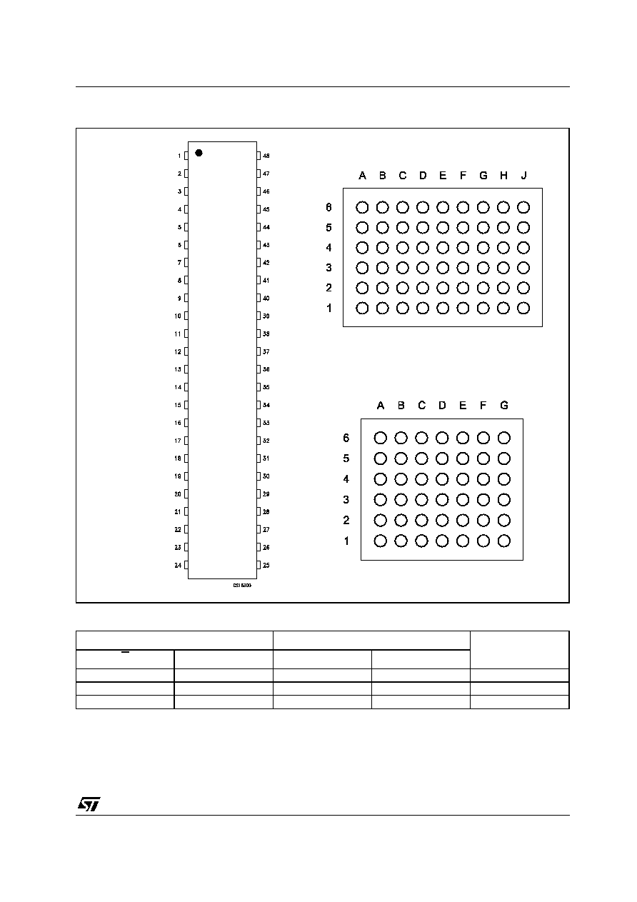
74VCXH1632245
16-BIT DUAL SUPPLY BUS TRANSCEIVER
LEVEL TRANSLATOR WITH A SIDE SERIES RESISTOR
ORDER CODES
PACKAGE
T & R
TSSOP48
74VCXH1632245TTR
TFBGA54
74VCXH1632245LBR
µ
TFBGA42
74VCXH1632245TBR
TSSOP
µ
TFBGA
TFBGA
LOGIC DIAGRAM
n = 1, 2
Rev. 1

74VCXH1632245
2/17
Figure 1: Input And Output Equivalent Circuit
Table 1: Pin Description
TFBGA54 PIN N∞
µ
TFBGA42 PIN N∞
TSSOP PIN N∞
SYMBOL
NAME AND FUNCTION
A3
B3
1
1DIR
Directional Controls
J3
F3
24
2DIR
Directional Controls
A6, B5, B6, C5,
C6, D5, D6, E5
A4, A5, A6, B5,
B6, C5, C6, D5
47, 46, 44, 43,
41, 40, 38, 37
1A1 to 1A8
Data Inputs/Outputs
E6, F5, F6, G5,
G6, H5, H6, J6
D6, E5, E6, F5,
F6,G4, G5, G6
36, 35, 33, 32,
30, 29, 27, 26
2A1 to 2A8
Data Inputs/Outputs
A1, B2, B1, C2,
C1, D2, D1, E2
A3, A2, A1, B2,
B1, C2, C1, D2
2, 3, 5, 6,
8, 9, 11, 12
1B1 to 1B8
Data Inputs/Outputs
E1, F2, F1, G2,
G1, H2, H1, J1
D1, E2, E1, F2,
F1,G3, G2, G1
13, 14, 16, 17,
19, 20, 22, 23
2B1 to 2B8
Data Inputs/Outputs
J4
F4
25
2G
Output Enable Inputs
A4
B4
48
1G
Output Enable Inputs
D3, D4, E3, E4,
F3, F4
C3, C4, E3, E4
4, 10, 15, 21,
28, 34, 39, 45
GND
Ground (0V)
A2, A5, B3, B4,
H3, H4, J2, J5
-
-
NC
No Connected
C4, G4
D4
42, 31
V
CCA
Positive Supply Voltage
C3, G3
D3
7, 18
V
CCB
Positive Supply Voltage
74VCXH1632245
3/17
Figure 2: Pin Connection (top view for TSSOP, top through view for BGA)
Table 2: Truth Table
X=Don't care; Z=High Impedance
INPUTS
FUNCTION
OUTPUT
G
DIR
A BUS
B BUS
L
L
OUTPUT
INPUT
A = B
L
H
INPUT
OUTPUT
B = A
H
X
Z
Z
Z
TSSOP
TFBGA
µ
TFBGA

74VCXH1632245
4/17
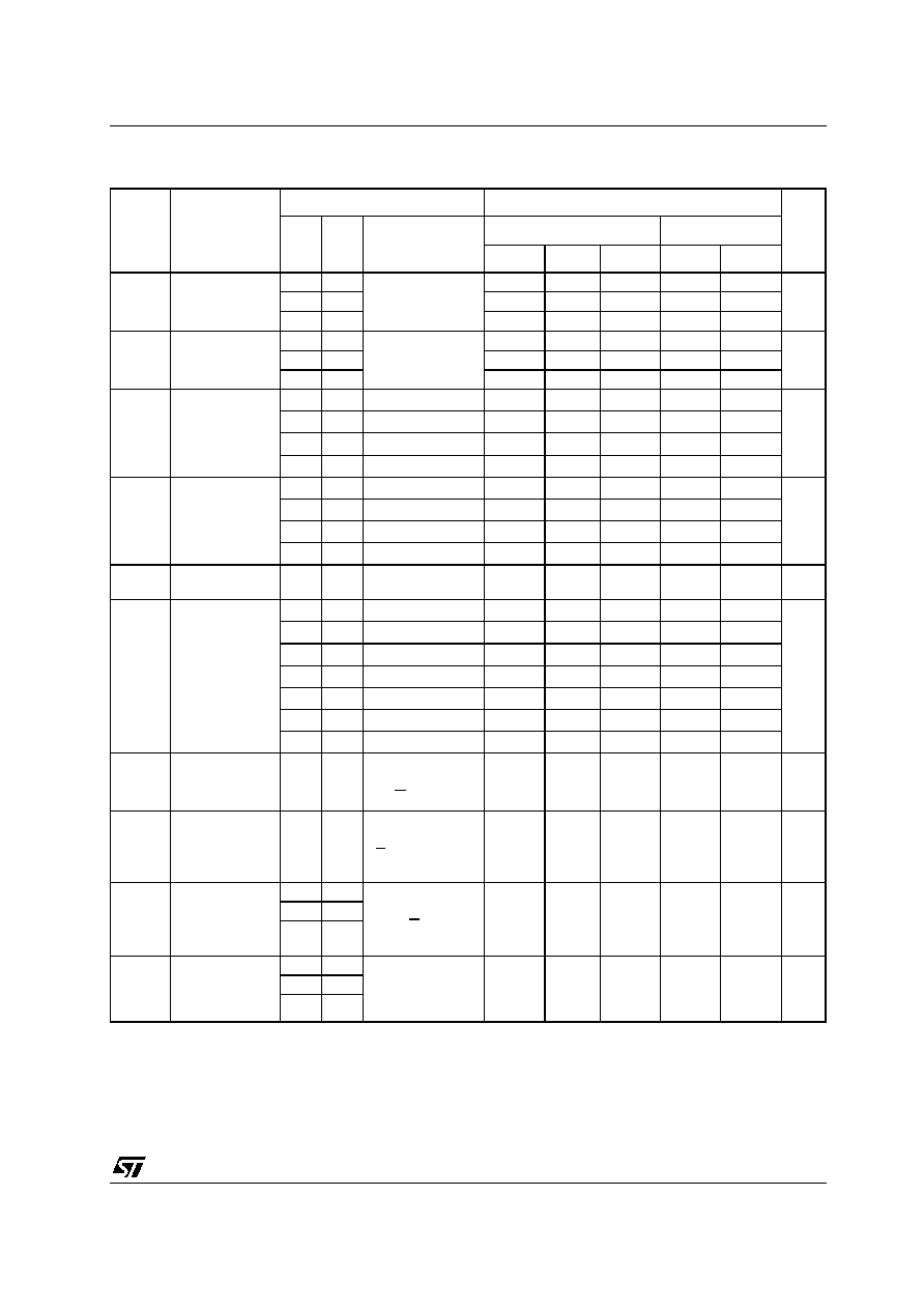
Table 3: Absolute Maximum Ratings
Absolute Maximum Ratings are those value beyond which damage to the device may occur. Functional operation under these conditions is
not implied
Table 4: Recommended Operating Conditions
1) V
IN
from 0.8V to 2.0V at V
CC
=3.0V
Symbol
Parameter
Value
Unit
V
CCA
Supply Voltage
-0.5 to +4.6
V
V
CCB
Supply Voltage
-0.5 to +4.6
V
V
I
DC Input Voltage
-0.5 to +4.6
V
V
I/OA
DC I/O Voltage (Output disabled)
-0.5 to +4.6
V
V
I/OB
DC I/O Voltage (Output disabled)
-0.5 to +4.6
V
V
I/OA
DC I/O Voltage
-0.5 to V
CCA
+ 0.5
V
V
I/OB
DC I/O Voltage
-0.5 to V
CCB
+ 0.5
V
I
IK
DC Input Diode Current
-
20
mA
I
OK
DC Output Diode Current
-
50
mA
I
OA
DC Output Current
±
50
mA
I
OB
DC Output Current
±
50
mA
I
CCA
DC V
CC
or Ground Current
±
100
mA
I
CCB
DC V
CC
or Ground Current
±
100
mA
P
d
Power Dissipation
400
mW
T
stg
Storage Temperature
-65 to +150
∞C
T
L
Lead Temperature (10 sec)
260
∞C
Symbol
Parameter
Value
Unit
V
CCA
Supply Voltage
2.3 to 3.6
V
V
CCB
Supply Voltage
1.65 to V
CCA
V
V
I
Input Voltage (Dir, G)
0 to V
CCB
V
V
I/OA
I/O Voltage
0 to V
CCA
V
V
I/OB
I/O Voltage
0 to V
CCB
V
T
op
Operating Temperature
-40 to 85
∞C
dt/dv
Input Rise and Fall Time (note 1)
0 to 10
ns/V
74VCXH1632245
5/17
Table 5: DC Specification For V
CCA
(*) V
CC
range = 3.3±0.3; 2.5±0.2V; 1.8±0.15V
Symbol
Parameter
Test Condition
Value
Unit
V
CCB
(*)
(V)
V
CCA
(*)
(V)
T
A
= 25 ∞C
-40 to 85 ∞C
Min.
Typ.
Max.
Min.
Max.
V
IHA
High Level Input
Voltage (An)
1.8
2.5
1.6
1.6
V
1.8
3.3
2.0
2.0
2.5
3.3
2.0
2.0
V
ILA
Low Level Input
Voltage (An)
1.8
2.5
0.7
0.7
V
1.8
3.3
0.8
0.8
2.5
3.3
0.8
0.8
V
OHA
High Level
Output Voltage
2.3
3.0
I
O
=-100
µ
A
2.8
2.8
V
2.3
3.0
I
O
=-8mA
2.4
2.4
1.65
3.0
I
O
=-8mA
2.4
2.4
1.65
2.3
I
O
=-6mA
1.8
1.8
V
OLA
Low Level
Output Voltage
2.3
3.0
I
O
=100
µ
A
0.2
0.2
V
2.3
3.0
I
O
=8mA
0.55
0.55
1.65
3.0
I
O
=8mA
0.55
0.55
1.65
2.3
I
O
=6mA
0.40
0.40
I
IA
Input Leakage
Current
2.7
3.6
V
I
= V
CC
or GND
±
0.5
±
5
µ
A
I
IA(HOLD)
Input Hold
Current
1.65
2.3
V
I
= 0.7 V
45
45
µ
A
1.65
2.3
V
I
= 1.6 V
-45
-45
1.65
3.0
V
I
= 0.8 V
75
75
1.65
3.0
V
I
= 2.0 V
-75
-75
2.3
3.0
V
I
= 0.8 V
75
75
2.3
3.0
V
I
= 2.0 V
-75
-75
2.7
3.6
V
I
= 0 to 3.6 V
±
500
I
OZA
High Impedance
Output Leakage
Current
2.7
3.6
V
IA
= GND or 3.6V
V
IB
= V
IHB
or V
ILB
G = V
CCB
±
1.0
±
10
µ
A
I
OFF
Power Off
Leakage Current
0
0
V
IA
= GND to 3.6V
V
IB
= GND to 3.6V
G, Dir = GND to
3.6V
±
1.0
±
10
µ
A
I
CCtA
Quiescent
Supply Current
1.95
3.6
V
IA
=V
CCA
or GND
V
IB
=V
CCB
or GND
Dir or G=V
CCB
or
GND
2
20
µ
A
1.95
2.7
2.7
3.6
I
CCtA
Maximum
Quiescent
Supply Current /
Input (An)
2.7
3.6
V
IA
=V
CCA
- 0.6V
V
IB
=V
CCB
or GND
0.75
mA
1.95
3.6
1.95
2.7