1/10
July 2003
s
HIGH SPEED: t
PD
= 4.0 ns (TYP.) at V
CC
= 5V
s
LOW POWER DISSIPATION:
I
CC
= 4
µ
A (MAX.) at T
A
=25∞C
s
HIGH NOISE IMMUNITY
V
NIH
=V
NIL
= 28% VCC (MIN.)
s
POWER DOWN PROTECTION ON INPUTS
& OUTPUTS
s
SYMMETRICAL OUTPUT IMPEDANCE:
|I
OH
| = I
OL
= 8 mA (MIN)
s
BALANCED PROPAGATION DELAYS:
t
PLH
t
PHL
s
OPERATING VOLTAGE RANGE:
V
CC
(OPR) = 2V to 5.5V
s
IMPROVED LATCH-UP IMMUNITY
s
LOW NOISE: V
OLP
= 0.9V (MAX.)
DESCRIPTION
The 74VHC16245 is an advanced high-speed
CMOS 16-BIT BUS TRANSCEIVER (3-STATE)
fabricated
with
sub-micron silicon gate and
double-layer metal wiring C
2
MOS technology.
This IC is intended for two-way asynchronous
communication
between
data
busses;
the
direction of data transmission is determined by
DIR input. The enable input G can be used to
disable the device so that the busses are
effectively isolated.
All
inputs
and
outputs
are
equipped
with
protection circuits against static discharge, giving
them 2KV ESD immunity and transient excess
voltage.
All floating bus terminals during High Z State must
be held HIGH or LOW.
74VHC16245
16-BIT BUS TRANSCEIVER
WITH 3-STATE OUTPUTS (NON INVERTED)
ORDER CODES
PACKAGE
TUBE
T & R
TSSOP
74VHC16245TTR
TSSOP
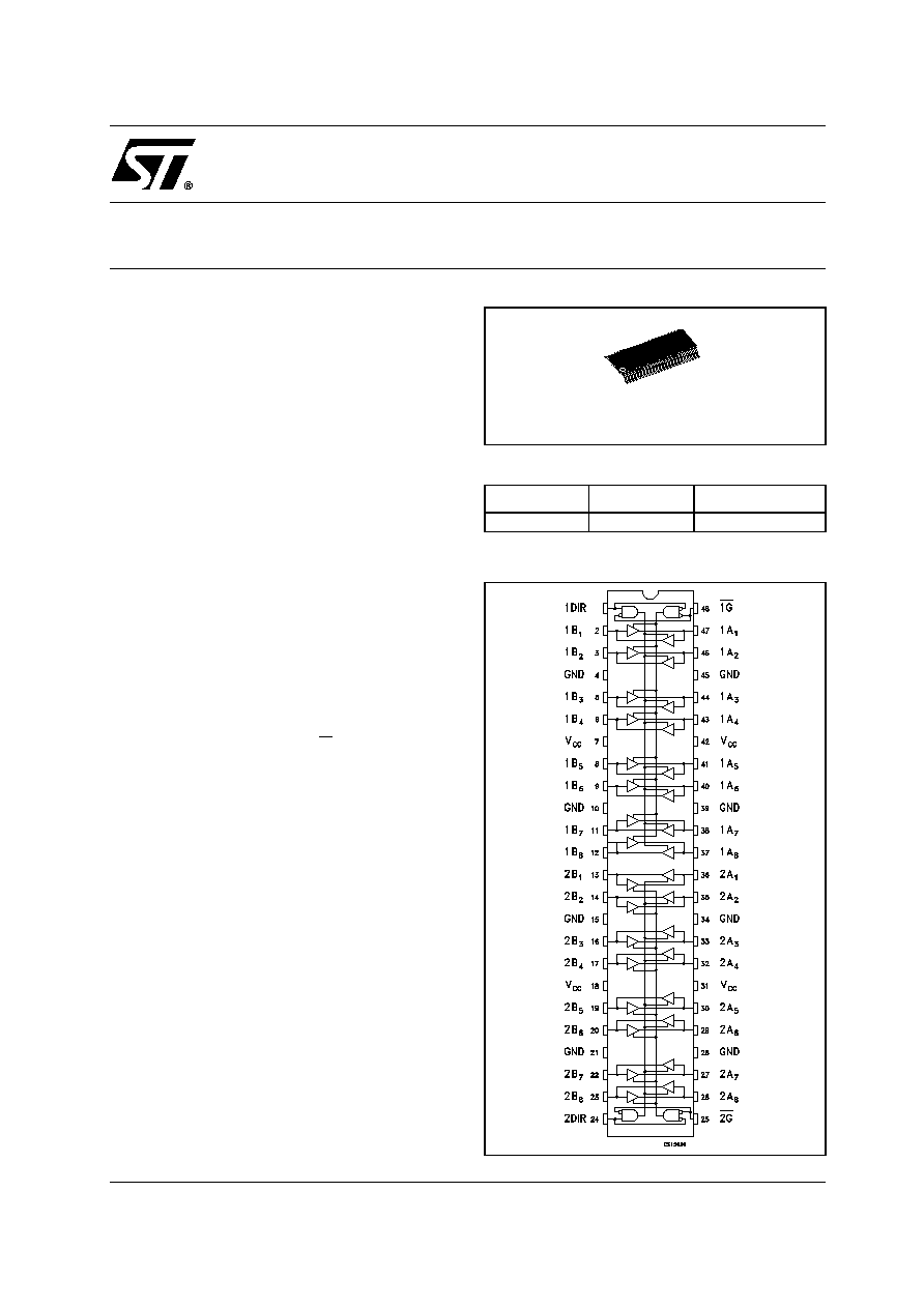
PIN CONNECTION
74VHC16245
2/10
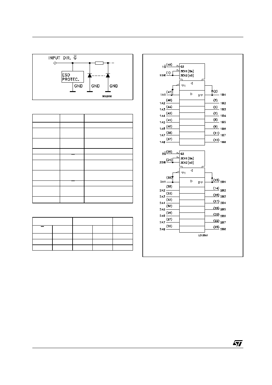
INPUT EQUIVALENT CIRCUIT
PIN DESCRIPTION
TRUTH TABLE
X : Don`t Care
Z : High Impedance
IEC LOGIC SYMBOLS
PIN No
SYMBOL
NAME AND FUNCTION
1
1DIR
Directional Control
2, 3, 5, 6, 8, 9,
11, 12
1B1 to 1B8 Data Inputs/Outputs
13, 14, 16, 17,
19, 20, 22, 23
2B1 to 2B8 Data Inputs/Outputs
24
2DIR
Directional Control
25
2G
Output Enable Input
36, 35, 33, 32,
30, 29, 27, 26
2A1 to 2A8 Data Inputs/Outputs
47, 46, 44, 43,
41, 40, 38, 38
1A1 to 1A8 Data Inputs/Outputs
48
1G
Output Enable Input
4, 10, 15, 21,
28, 34, 39, 45
GND
Ground (0V)
7, 18, 31, 42
V
CC
Positive Supply Voltage
INPUTS
FUNCTION
OUTPUT
G
DIR
A BUS
B BUS
Yn
L
L
OUTPUT
INPUT
A = B
L
H
INPUT
OUTPUT
B = A
H
X
Z
Z
Z
74VHC16245
3/10
ABSOLUTE MAXIMUM RATINGS
Absolute Maximum Ratings are those values beyond which damage to the device may occur. Functional operation under these conditions is
not implied
RECOMMENDED OPERATING CONDITIONS
1) V
IN
from 30% to 70% of V
CC
Symbol
Parameter
Value
Unit
V
CC
Supply Voltage
-0.5 to +7.0
V
V
I
DC Input Voltage (DIR, G)
-0.5 to +7.0
V
V
I/O
Bus I/O Voltage
-0.5 to V
CC
+ 0.5
V
V
O
DC Output Voltage
-0.5 to V
CC
+ 0.5
V
I
IK
DC Input Diode Current
- 20
mA
I
OK
DC Output Diode Current
±
20
mA
I
O
DC Output Current
±
25
mA
I
CC
or I
GND
DC V
CC
or Ground Current
±
75
mA
T
stg
Storage Temperature
-65 to +150
∞C
T
L
Lead Temperature (10 sec)
300
∞C
Symbol
Parameter
Value
Unit
V
CC
Supply Voltage
2 to 5.5
V
V
I
Input Voltage (DIR, G)
0 to 5.5
V
V
I/O
Bus I/O Voltage
0 to V
CC
V
V
O
Output Voltage
0 to V
CC
V
T
op
Operating Temperature
-55 to 125
∞C
dt/dv
Input Rise and Fall Time (note 1) (V
CC
= 3.3
±
0.3V)
(V
CC
= 5.0
±
0.5V)
0 to 100
0 to 20
ns/V
74VHC16245
4/10
DC SPECIFICATIONS
Symbol
Parameter
Test Condition
Value
Unit
V
CC
(V)
T
A
= 25∞C
-40 to 85∞C
-55 to 125∞C
Min.
Typ.
Max.
Min.
Max.
Min.
Max.
V
IH
High Level Input
Voltage
2.0
1.5
1.5
1.5
V
3.0 to
5.5
0.7V
CC
0.7V
CC
0.7V
CC
V
IL
Low Level Input
Voltage
2.0
0.5
0.5
0.5
V
3.0 to
5.5
0.3V
CC
0.3V
CC
0.3V
CC
V
OH
High Level Output
Voltage
2.0
I
O
=-50
µ
A
1.9
2.0
1.9
1.9
V
3.0
I
O
=-50
µ
A
2.9
3.0
2.9
2.9
4.5
I
O
=-50
µ
A
4.4
4.5
4.4
4.4
3.0
I
O
=-4 mA
2.58
2.48
2.4
4.5
I
O
=-8 mA
3.94
3.8
3.7
V
OL
Low Level Output
Voltage
2.0
I
O
=50
µ
A
0.0
0.1
0.1
0.1
V
3.0
I
O
=50
µ
A
0.0
0.1
0.1
0.1
4.5
I
O
=50
µ
A
0.0
0.1
0.1
0.1
3.0
I
O
=4 mA
0.36
0.44
0.55
4.5
I
O
=8 mA
0.36
0.44
0.55
Ioz
High Impedance
Output Leakage
Current
5.5
V
I
= V
IH
or V
IL
V
O
= V
CC
or GND
±
0.25
±
2.5
±
2.5
µ
A
I
I
Input Leakage
Current
0 to
5.5
V
I
= 5.5V or GND
±
0.1
±
1
±
1
µ
A
I
CC
Quiescent Supply
Current
5.5
V
I
= V
CC
or GND
4
40
40
µ
A

74VHC16245
5/10
AC ELECTRICAL CHARACTERISTICS (Input t
r
= t
f
= 3ns)
(*) Voltage range is 3.3V
±
0.3V
(**) Voltage range is 5.0V
±
0.5V
Note 1: Parameter guaranteed by design. t
soLH
= |t
pLHm
- t
pLHn
|, t
soHL
= |t
pHLm
- t
pHLn
|
CAPACITIVE CHARACTERISTICS
1) C
PD
is defined as the value of the IC's internal equivalent capacitance which is calculated from the operating current consumption without
load. (Refer to Test Circuit). Average operating current can be obtained by the following equation. I
CC(opr)
= C
PD
x V
CC
x f
IN
+ I
CC
/8 (per circuit)
Symbol
Parameter
Test Condition
Value
Unit
V
CC
(V)
C
L
(pF)
T
A
= 25∞C
-40 to 85∞C
-55 to 125∞C
Min.
Typ.
Max.
Min.
Max.
Min.
Max.
t
PLH
t
PHL
Propagation Delay
Time
3.3
(*)
15
5.8
8.4
1.0
10.0
1.0
10.0
ns
3.3
(*)
50
8.3
11.9
1.0
13.5
1.0
13.5
5.0
(**)
15
4.0
5.5
1.0
6.5
1.0
6.5
5.0
(**)
50
5.5
7.5
1.0
8.5
1.0
8.5
t
PZL
t
PZH
Output Disable
Time
3.3
(*)
15
R
L
= 1K
8.5
13.2
1.0
15.5
1.0
15.5
ns
3.3
(*)
50
R
L
= 1K
11.0
16.7
1.0
19.0
1.0
19.0
5.0
(**)
15
R
L
= 1K
5.8
8.5
1.0
10.0
1.0
10.0
5.0
(**)
50
R
L
= 1K
7.3
10.6
1.0
12.0
1.0
12.0
t
PLZ
t
PHZ
Output Enable
Time
3.3
(*)
50
R
L
= 1K
11.5
15.8
1.0
18.0
1.0
18.0
ns
5.0
(**)
50
R
L
= 1K
7.0
9.7
1.0
11.0
1.0
11.0
t
OSLH
t
OSHL
Output to Output
Skew time (note 1)
3.3
(*)
50
1.5
1.5
1.5
ns
5.0
(**)
50
1.0
1.0
1.0
Symbol
Parameter
Test Condition
Value
Unit
T
A
= 25∞C
-40 to 85∞C
-55 to 125∞C
Min.
Typ.
Max.
Min.
Max.
Min.
Max.
C
IN
Input Capacitance
4
10
10
10
pF
C
I/O
Output
Capacitance
8
pF
C
PD
Power Dissipation
Capacitance
(note 1)
21
pF
74VHC16245
6/10
DYNAMIC SWITCHING CHARACTERISTICS
1) Worst case package.
2) Max number of outputs defined as (n). Data inputs are driven 0V to 5.0V, (n-1) outputs switching and one output at GND.
3) Max number of data inputs (n) switching. (n-1) switching 0V to 5.0V. Inputs under test switching: 5.0V to threshold (V
ILD
), 0V to threshold
(V
IHD
), f=1MHz.
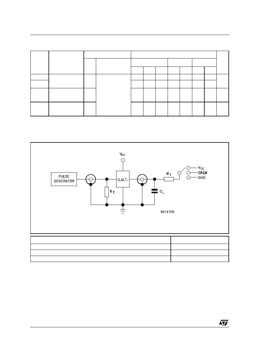
TEST CIRCUIT
C
L
=15/ 50pF or equivalent (includes jig and probe capacitance)
R
L
= R
1
= 1K
or equivalent
R
T
= Z
OUT
of pulse generator (typically 50
Symbol
Parameter
Test Condition
Value
Unit
V
CC
(V)
T
A
= 25∞C
-40 to 85∞C
-55 to 125∞C
Min.
Typ.
Max.
Min.
Max.
Min.
Max.
V
OLP
Dynamic Low
Voltage Quiet
Output (note 1, 2)
5.0
C
L
= 50 pF
0.6
0.9
V
V
OLV
-0.9
-0.6
V
IHD
Dynamic High
Voltage Input
(note 1, 3)
5.0
3.5
V
V
ILD
Dynamic Low
Voltage Input
(note 1, 3)
5.0
1.5
V
TEST
SWITCH
t
PLH
, t
PHL
Open
t
PZL
, t
PLZ
V
CC
t
PZH
, t
PHZ
GND
74VHC16245
7/10
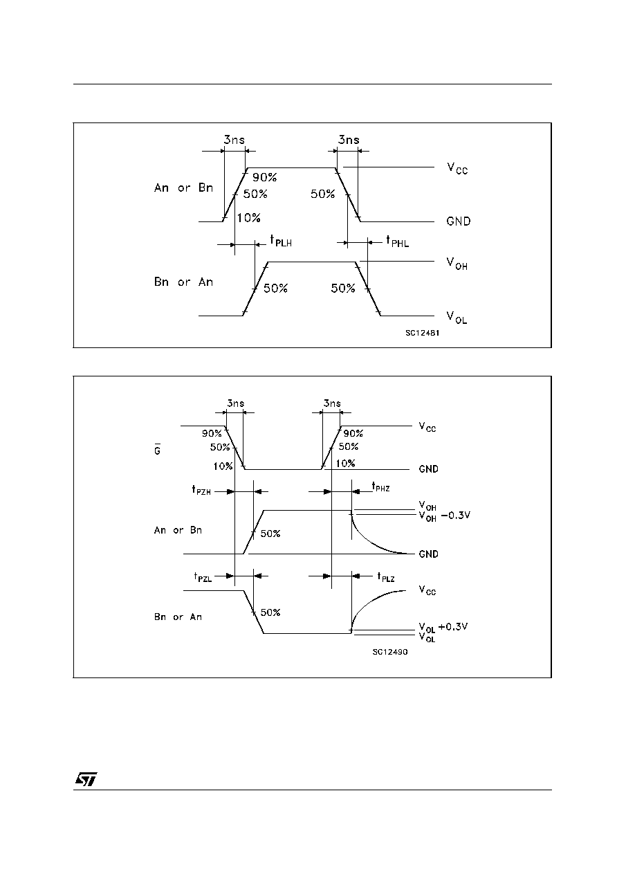
WAVEFORM 1: PROPAGATION DELAYS (f=1MHz; 50% duty cycle)
WAVEFORM 2: OUTPUT ENABLE AND DISABLE TIME (f=1MHz; 50% duty cycle)
74VHC16245
8/10
DIM.
mm.
inch
MIN.
TYP
MAX.
MIN.
TYP.
MAX.
A
1.2
0.047
A1
0.05
0.15
0.002
0.006
A2
0.9
0.035
b
0.17
0.27
0.0067
0.011
c
0.09
0.20
0.0035
0.0079
D
12.4
12.6
0.488
0.496
E
8.1 BSC
0.318 BSC
E1
6.0
6.2
0.236
0.244
e
0.5 BSC
0.0197 BSC
K
0∞
8∞
0∞
8∞
L
0.50
0.75
0.020
0.030
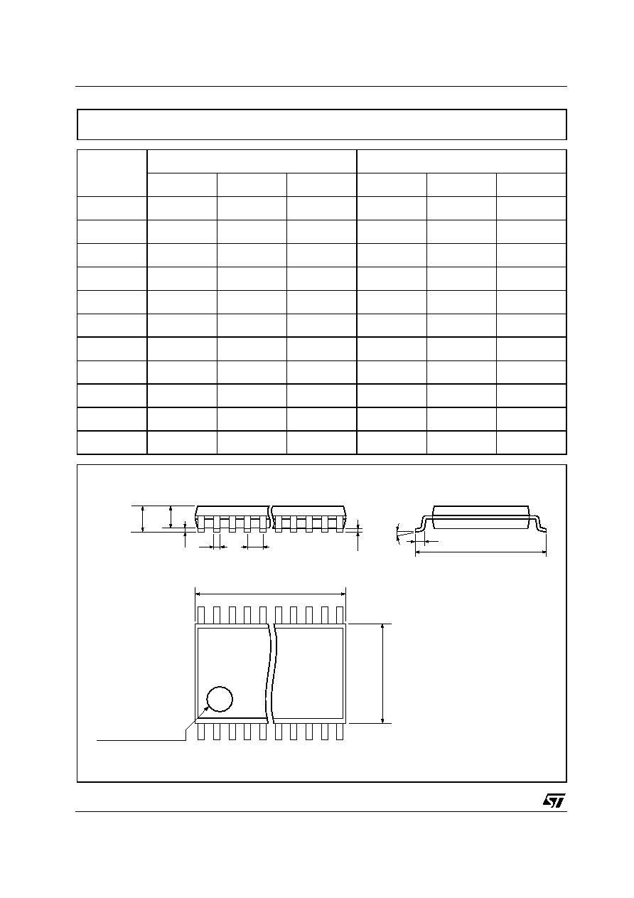
TSSOP48 MECHANICAL DATA
c
E
b
A2
A
E1
D
1
PIN 1 IDENTIFICATION
A1
L
K
e
7065588C
74VHC16245
9/10
DIM.
mm.
inch
MIN.
TYP
MAX.
MIN.
TYP.
MAX.
A
330
12.992
C
12.8
13.2
0.504
0.519
D
20.2
0.795
N
60
2.362
T
30.4
1.197
Ao
8.7
8.9
0.343
0.350
Bo
13.1
13.3
0.516
0.524
Ko
1.5
1.7
0.059
0.067
Po
3.9
4.1
0.153
0.161
P
11.9
12.1
0.468
0.476
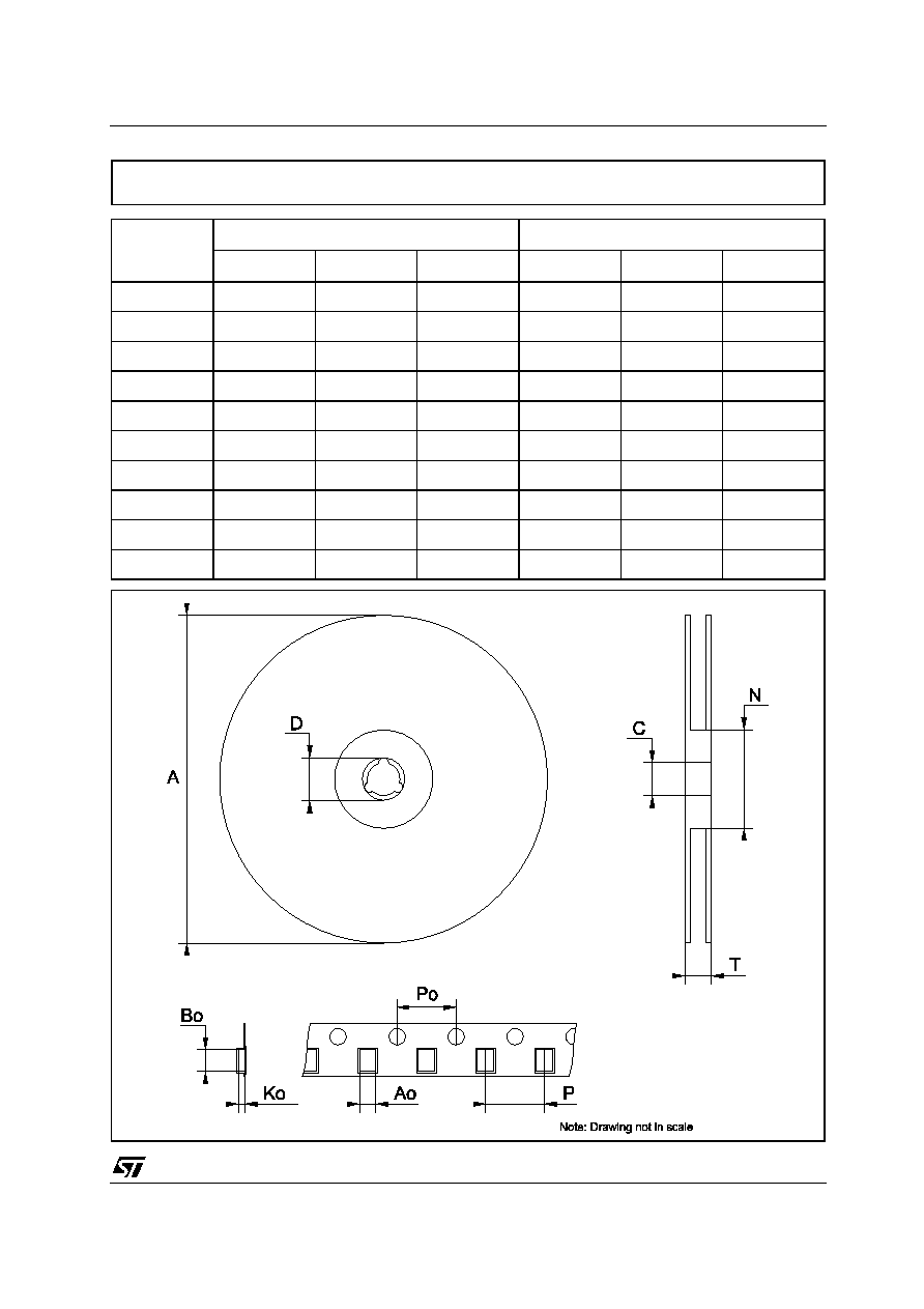
Tape & Reel TSSOP48 MECHANICAL DATA

74VHC16245
10/10
Information furnished is believed to be accurate and reliable. However, STMicroelectronics assumes no responsibility for the
consequences of use of such information nor for any infringement of patents or other rights of third parties which may result from
its use. No license is granted by implication or otherwise under any patent or patent rights of STMicroelectronics. Specifications
mentioned in this publication are subject to change without notice. This publication supersedes and replaces all information
previously supplied. STMicroelectronics products are not authorized for use as critical components in life support devices or
systems without express written approval of STMicroelectronics.
© The ST logo is a registered trademark of STMicroelectronics
© 2003 STMicroelectronics - Printed in Italy - All Rights Reserved
STMicroelectronics GROUP OF COMPANIES
Australia - Brazil - Canada - China - Finland - France - Germany - Hong Kong - India - Israel - Italy - Japan - Malaysia - Malta - Morocco
Singapore - Spain - Sweden - Switzerland - United Kingdom - United States.
© http://www.st.com