 | –≠–ª–µ–∫—Ç—Ä–æ–Ω–Ω—ã–π –∫–æ–º–ø–æ–Ω–µ–Ω—Ç: 74VHC273T | –°–∫–∞—á–∞—Ç—å:  PDF PDF  ZIP ZIP |
74VHC273
OCTAL D-TYPE FLIP FLOP WITH CLEAR
PRELIMINARY DATA
October 1999
s
HIGH SPEED:
f
MAX
= 165 MHz (TYP.) at V
CC
= 5V
s
LOW POWER DISSIPATION:
I
CC
= 4
µ
A (MAX.) at T
A
= 25
o
C
s
HIGH NOISE IMMUNITY:
V
NIH
= V
NIL
= 28% V
CC
(MIN.)
s
POWER DOWN PROTECTION ON INPUTS
s
SYMMETRICAL OUTPUT IMPEDANCE:
|I
OH
| = I
OL
= 8 mA (MIN)
s
BALANCED PROPAGATION DELAYS:
t
PLH
t
PHL
s
OPERATING VOLTAGE RANGE:
V
CC
(OPR) = 2V to 5.5V
s
PIN AND FUNCTION COMPATIBLE WITH
74 SERIES 273
s
IMPROVED LATCH-UP IMMUNITY
s
LOW NOISE V
OLP
= 0.9V (Max.)
DESCRIPTION
The 74VHC273 is an advanced high-speed
CMOS OCTAL
D-TYPE FLIP FLOP WITH
CLEAR fabricated with sub-micron silicon gate
and
double-layer
metal
wiring
C
2
MOS
technology.
Information signals applied to D inputs are
transfered to the Q outputs on the positive going
edge of the clock pulse.
When the CLEAR input is held low, the Q outputs
are held low independently of the other inputs .
Power down protection is provided on all inputs
and 0 to 7V can be accepted on inputs with no
regard to the supply voltage. This device can be
used to interface 5V to 3V.
All inputs
and
outputs are
equipped with
protection circuits against static discharge, giving
them 2KV ESD immunity and transient excess
voltage.
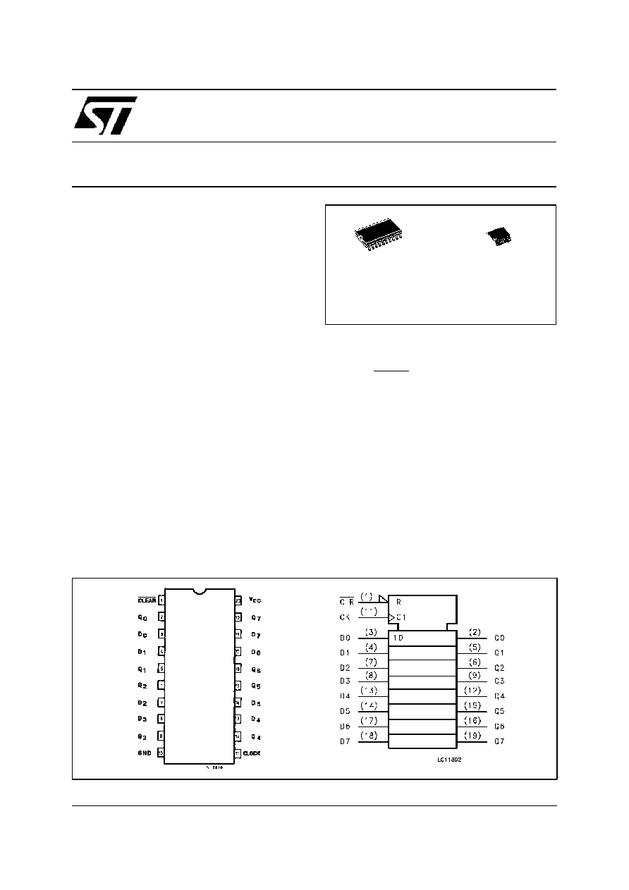
PIN CONNECTION AND IEC LOGIC SYMBOLS
ORDER CODES :
74VHC273M
74VHC273T
M
(Micro Package)
T
(TSSOP Package)
Æ
1/10
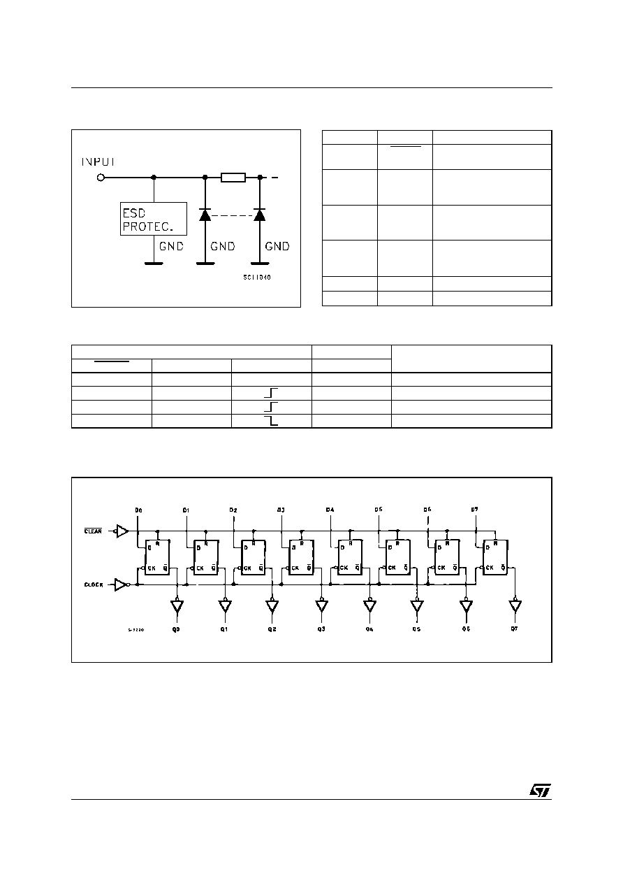
INPUT EQUIVALENT CIRCUIT
LOGIC DIAGRAMS
PIN DESCRIPTION
PIN No
SYMBOL
NAME AND FUNCT ION
1
CLEAR
Asyncronous Master
Reset (Active LOW)
2, 5, 6, 9,
12, 15, 16,
19
Q0 to Q7
Flip-Flop Outputs
3, 4, 7, 8,
13, 14, 17,
18
D0 to D7
Data Inputs
11
CLOCK
Clock Input
(LOW-to-HIGH, Edge-
Triggered)
10
GND
Ground (0V)
20
V
CC
Positive Supply Voltage
TRUTH TABLE
I NPUTS
OUT PUT S
F UNCTIO N
CL EAR
D
CLO CK
Q
L
X
X
L
CLEAR
H
L
L
H
H
H
H
X
Q
n
NO CHANGE
X:Don't Care
Thislogic diagram has notbe used to esimate propagation delays
74VHC273
2/10
ABSOLUTE MAXIMUM RATINGS
Symbol
Parameter
Val ue
Unit
V
CC
Supply Voltage
-0.5 to +7.0
V
V
I
DC Input Voltage
-0.5 to +7.0
V
V
O
DC Output Voltage
-0.5 to V
CC
+ 0.5
V
I
IK
DC Input Diode Current
- 20
mA
I
OK
DC Output Diode Current
±
20
mA
I
O
DC Output Current
±
25
mA
I
CC
or I
GND
DC V
CC
or Ground Current
±
75
mA
T
stg
Storage Temperature
-65 to +150
o
C
T
L
Lead Temperature (10 sec)
300
o
C
Absolute Maximum Ratings are those values beyond which damage to the device may occur. Functional operation under these condition is not implied.
RECOMMENDED OPERATING CONDITIONS
Symbol
Parameter
Valu e
Uni t
V
CC
Supply Voltage
2.0 to 5.5
V
V
I
Input Voltage
0 to 5.5
V
V
O
Output Voltage
0 to V
CC
V
T
op
Operating Temperature
-40 to +85
o
C
dt/dv
Input Rise and Fall Time (see note 1) (V
CC
= 3.3
±
0.3V)
(V
CC
= 5.0
±
0.5V)
0 to 100
0 to 20
ns/V
ns/V
1) V
IN
from 30% to70%of V
CC
DC SPECIFICATIONS
Symb ol
Parameter
T est Cond ition s
Val ue
Un it
V
CC
(V)
T
A
= 25
o
C
-40 to 85
o
C
Min.
Typ .
Max.
Min .
Max.
V
IH
High Level Input
Voltage
2.0
1.5
1.5
V
3.0 to 5.5
0.7V
CC
0.7V
CC
V
IL
Low Level Input
Voltage
2.0
0.5
0.5
V
3.0 to 5.5
0.3V
CC
0.3V
CC
V
OH
High Level Output
Voltage
2.0
I
O
=-50
µ
A
1.9
2.0
1.9
V
3.0
I
O
=-50
µ
A
2.9
3.0
2.9
4.5
I
O
=-50
µ
A
4.4
4.5
4.4
3.0
I
O
=-4 mA
2.58
2.48
4.5
I
O
=-8 mA
3.94
3.8
V
OL
Low Level Output
Voltage
2.0
I
O
=50
µ
A
0.0
0.1
0.1
V
3.0
I
O
=50
µ
A
0.0
0.1
0.1
4.5
I
O
=50
µ
A
0.0
0.1
0.1
3.0
I
O
=4 mA
0.36
0.44
4.5
I
O
=8 mA
0.36
0.44
I
I
Input Leakage Current
0 to 5.5
V
I
= 5.5V or GND
±
0.1
±
1.0
µ
A
I
CC
Quiescent Supply
Current
5.5
V
I
= V
CC
or GND
4
40
µ
A
74VHC273
3/10
CAPACITIVE CHARACTERISTICS
Symb ol
Parameter
T est Cond ition s
Val ue
Un it
T
A
= 25
o
C
-40 to 85
o
C
Min.
Typ .
Max.
Min .
Max.
C
IN
Input Capacitance
4
10
10
pF
C
PD
Power Dissipation
Capacitance (note 1)
31
pF
1) C
PD
isdefined as the value of the IC'sinternal equivalent capacitance which is calculated fromthe operating current consumption without load. (Referto
Test Circuit).Average operating current can be obtained by the following equation. I
CC
(opr) = C
PD
∑
V
CC
∑
f
IN
+ I
CC
/8 (per Flip-Flop)
AC ELECTRICAL CHARACTERISTICS (Input t
r
= t
f
=3 ns)
Symb ol
Parameter
Test Co nditi on
Val ue
Un it
V
CC
(V)
C
L
(pF )
T
A
= 25
o
C
-40 to 85
o
C
Min.
Typ .
Max.
Min .
Max.
t
PLH
t
PHL
Propagation Delay
Time
CK to Q
3.3
(*)
15
8.7
13.6
1.0
16.0
ns
3.3
(*)
50
11.2
17.1
1.0
19.5
5.0
(**)
15
5.8
9.0
1.0
10.5
5.0
(**)
50
7.3
11.0
1.0
12.5
t
PHL
Propagation Delay
Time
CLR to Q
3.3
(*)
15
8.9
13.6
1.0
16.0
ns
3.3
(*)
50
11.4
17.1
1.0
19.5
5.0
(**)
15
5.2
8.5
1.0
10.0
5.0
(**)
50
6.7
10.5
1.0
12.0
t
w
CLR pulse Width
LOW
3.3
(*)
5.0
6.0
ns
5.0
(**)
5.0
5.0
t
w
CK pulse Width
HIGH or LOW
3.3
(*)
5.5
6.5
ns
5.0
(**)
5.0
5.0
t
s
Setup Time D to CK
HIGH or LOW
3.3
(*)
5.5
6.5
ns
5.0
(**)
4.5
4.5
t
h
Hold Time D to CK
HIGH or LOW
3.3
(*)
1.0
1.0
ns
5.0
(**)
1.0
1.0
t
REM
Removal Time
CLR to CK
3.3
(*)
2.5
2.5
ns
5.0
(**)
2.0
2.0
f
MAX
Maximum Clock
Frequency
3.3
(*)
15
75
120
65
MHz
3.3
(*)
50
50
75
45
5.0
(**)
15
120
165
100
5.0
(**)
50
80
110
70
t
OSLH
t
OSHL
Output to Output Skew
Time (note 1)
3.3
(*)
50
1.5
1.5
ns
5.0
(**)
50
1.0
1.0
(*) Voltage range is 3.3V
±
0.3V
(**) Voltage range is 5V
±
0.5V
Note 1: Parameter guaranteed by design. t
soLH
= |t
pLHm
- t
pLHn
|, t
soHL
= |t
pHLm
- t
pHLn
|
74VHC273
4/10
DYNAMIC SWITCHING CHARACTERISTICS
Symb ol
Parameter
T est Cond ition s
Val ue
Un it
V
CC
(V)
T
A
= 25
o
C
-40 to 85
o
C
Min.
Typ .
Max.
Min .
Max.
V
OLP
Dynamic Low Voltage
Quiet Output (note 1, 2)
5.0
C
L
= 50 pF
0.6
0.9
V
V
OLV
-0.9
-0.6
V
IHD
Dynamic High Voltage
Input (note 1, 3)
5.0
3.5
V
IL D
Dynamic Low Voltage
Input (note 1, 3)
5.0
1.5
1) Worst case package.
2) Max number of outputs defined as (n). Data inputs are driven 0V to 5.0V, (n -1) outputs switching and one output at GND.
3) Max number of data inputs (n) switching. (n-1) switching 0V to5.0V. Inputs under test switching: 5.0V to threshold (V
ILD
), 0V to threshold (V
IHD
), f=1MHz.
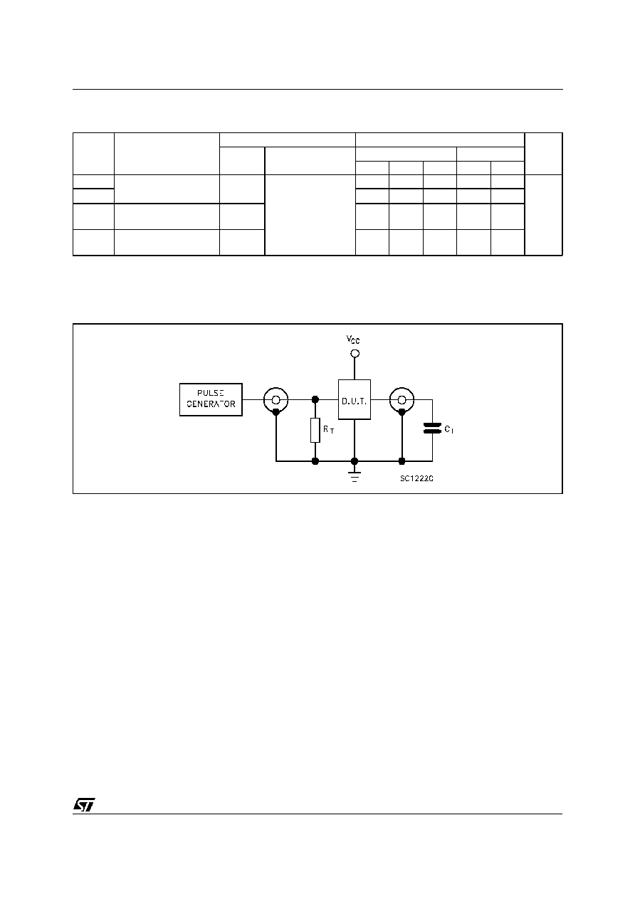
TEST CIRCUIT
C
L
= 15/50 pF or equivalent (includes jig and probe capacitance)
R
T
= Z
OUT
of pulse generator (typically 50
)
74VHC273
5/10
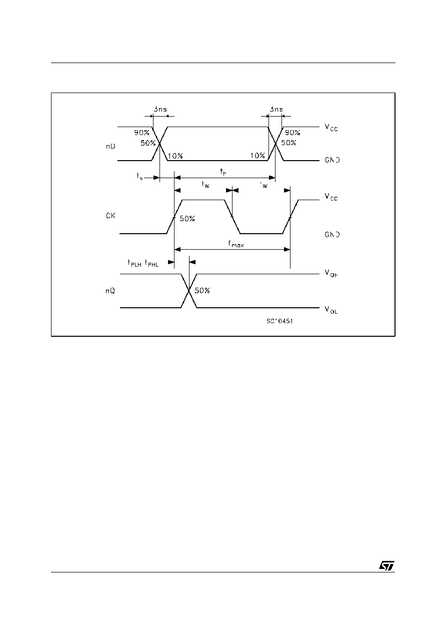
WAVEFORM 1: PROPAGATION DELAYS, SETUP AND HOLD TIMES (f=1MHz; 50% duty cycle)
74VHC273
6/10
WAVEFORM 2: PROPAGATION DELAYS (f=1MHz; 50% duty cycle)
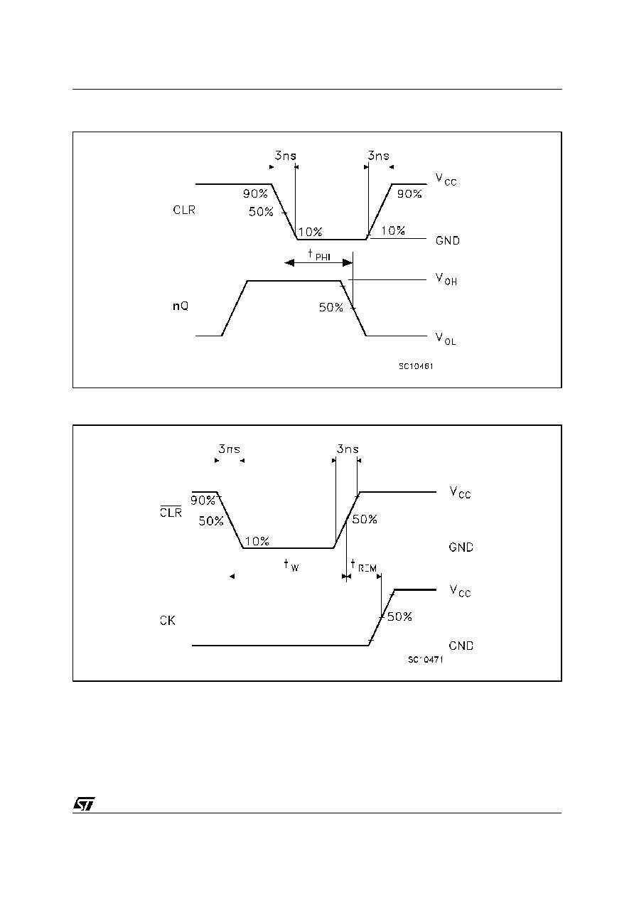
WAVEFORM 3: RECOVERY TIME (f=1MHz; 50% duty cycle)
74VHC273
7/10
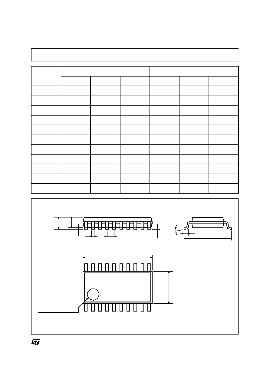
DIM.
mm
inch
MIN.
TYP.
MAX.
MIN.
TYP.
MAX.
A
2.65
0.104
a1
0.10
0.20
0.004
0.007
a2
2.45
0.096
b
0.35
0.49
0.013
0.019
b1
0.23
0.32
0.009
0.012
C
0.50
0.020
c1
45 (typ.)
D
12.60
13.00
0.496
0.512
E
10.00
10.65
0.393
0.419
e
1.27
0.050
e3
11.43
0.450
F
7.40
7.60
0.291
0.299
L
0.50
1.27
0.19
0.050
M
0.75
0.029
S
8 (max.)
P013L
SO-20 MECHANICAL DATA
74VHC273
8/10
DIM.
mm
inch
MIN.
TYP.
MAX.
MIN.
TYP.
MAX.
A
1.1
0.433
A1
0.05
0.10
0.15
0.002
0.004
0.006
A2
0.85
0.9
0.95
0.335
0.354
0.374
b
0.19
0.30
0.0075
0.0118
c
0.09
0.2
0.0035
0.0079
D
6.4
6.5
6.6
0.252
0.256
0.260
E
6.25
6.4
6.5
0.246
0.252
0.256
E1
4.3
4.4
4.48
0.169
0.173
0.176
e
0.65 BSC
0.0256 BSC
K
0
o
4
o
8
o
0
o
4
o
8
o
L
0.50
0.60
0.70
0.020
0.024
0.028
c
E
b
A2
A
E1
D
1
PIN 1 IDENTIFICATION
A1
L
K
e
TSSOP20 MECHANICAL DATA
74VHC273
9/10

Information furnished is believed to be accurate and reliable. However, STMicroelectronics assumes no responsibility for the consequences
of use of such information nor for any infringement of patents or other rights of third parties which may result from its use. No license is
granted by implication or otherwise under any patent or patent rights of STMi croelectronics. Specification mentioned in this publication are
subject to change without notice. This publication supersedes and replaces all information previously supplied. STMi croelectronics products
are not authorized for use as critical components in life support devices or systems withoutexpress written approval of STMicroelectronics.
The ST logo is a registered trademark of STMicroelectronics
©
1999 STMicroelectronics ≠ Printed in Italy ≠ All Rights Reserved
STMicroelectronics GROUP OF COMPANIES
Australia - Brazil - China - Finland - France - Germany - Hong Kong - India - Italy - Japan - Malaysia - Malta - Morocco
Singapore - Spain - Sweden - Switzerland - United Kingdom - U.S.A.
http://www.st.com
.
74VHC273
10/10