74VHCT157A
QUAD 2 CHANNEL MULTIPLEXER
PRELIMINARY DATA
March 2000
s
HIGH SPEED: t
PD
= 6.2 ns (TYP.) at V
CC
= 5V
s
LOW POWER DISSIPATION:
I
CC
= 4
µ
A (MAX.) at T
A
= 25
o
C
s
COMPATIBLE WITH TTL OUTPUTS:
V
IH
= 2V (MIN), V
IL
= 0.8V (MAX)
s
POWER DOWN PROTECTION ON INPUTS &
OUTPUTS
s
SYMMETRICAL OUTPUT IMPEDANCE:
|I
OH
| = I
OL
= 8 mA (MIN)
s
BALANCED PROPAGATION DELAYS:
t
PLH
t
PHL
s
OPERATING VOLTAGE RANGE:
V
CC
(OPR) = 4.5V to 5.5V
s
PIN AND FUNCTION COMPATIBLE WITH
74 SERIES 157
s
IMPROVED LATCH-UP IMMUNITY
s
LOW NOISE: V
OLP
= 0.8V (Max.)
DESCRIPTION
The 74VHCT157A is an high-speed CMOS
QUAD 2-CHANNEL MULTIPLEXER fabricated
with sub-micron silicon gate and double-layer
metal wiring C
2
MOS technology.
It consists of four 2-input digital multiplexers with
common select and strobe inputs. It
is a
non-inverting multiplexer. When the STROBE
input is held high, selection of data is inhibited
and all the outputs become low. The SELECT
decoding determines whether the A or B inputs
get routed to their corresponding Y outputs.
Power down protection is provided on all inputs
and outputs and 0 to 7V can be accepted on
inputs with no regard to the supply voltage. This
device can be used to interface 5V to 3V.All
inputs and outputs are equipped with protection
circuits against static discharge, giving them 2KV
ESD immunity and transient excess voltage.
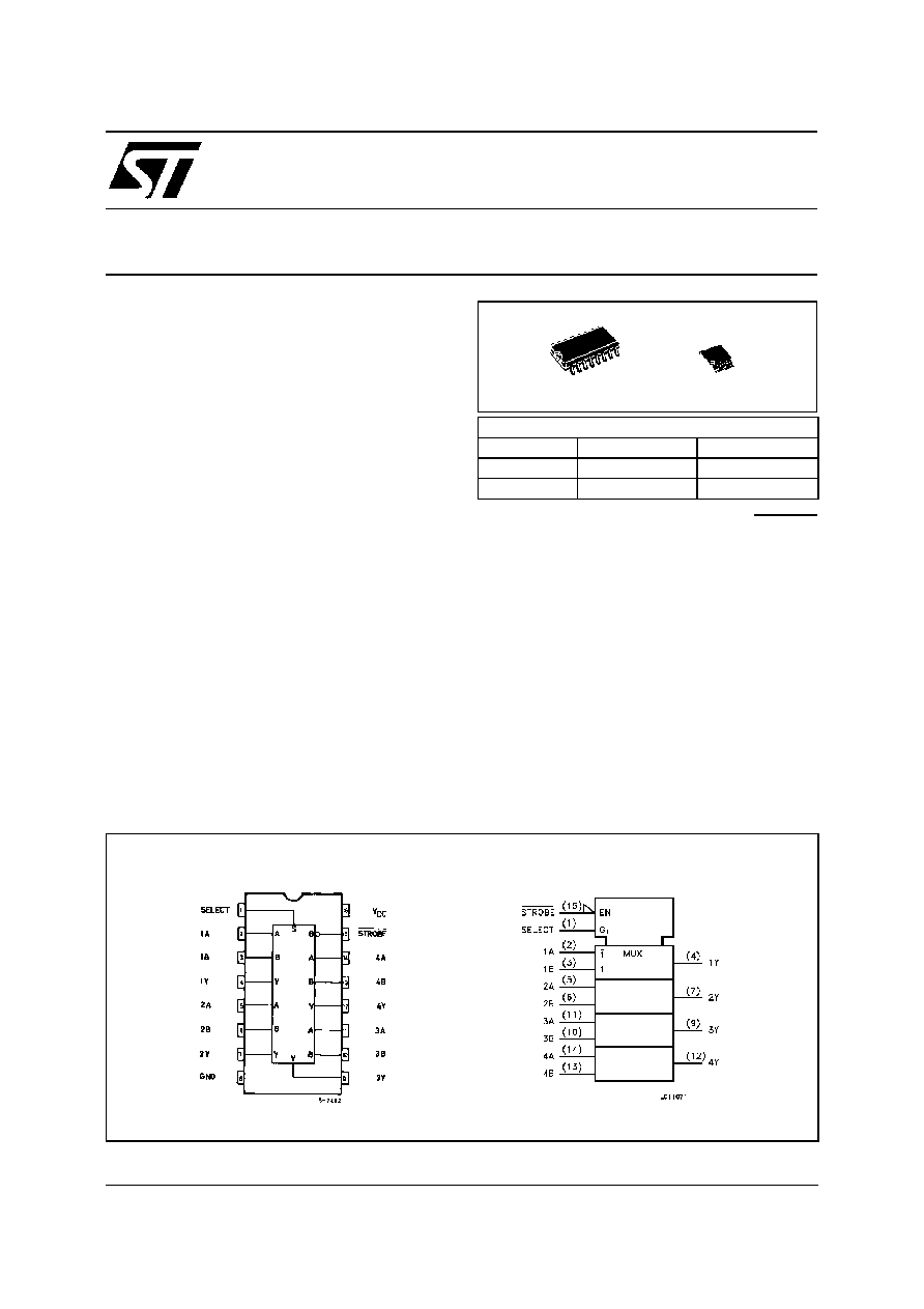
PIN CONNECTION AND IEC LOGIC SYMBOLS
Æ
SOP
TSSOP
ORDER CODES
PACKAGE
T UBE
T & R
SOP
74VHCT157AM
74VHCT157AMTR
TSSOP
74VHCT157ATTR
1/9
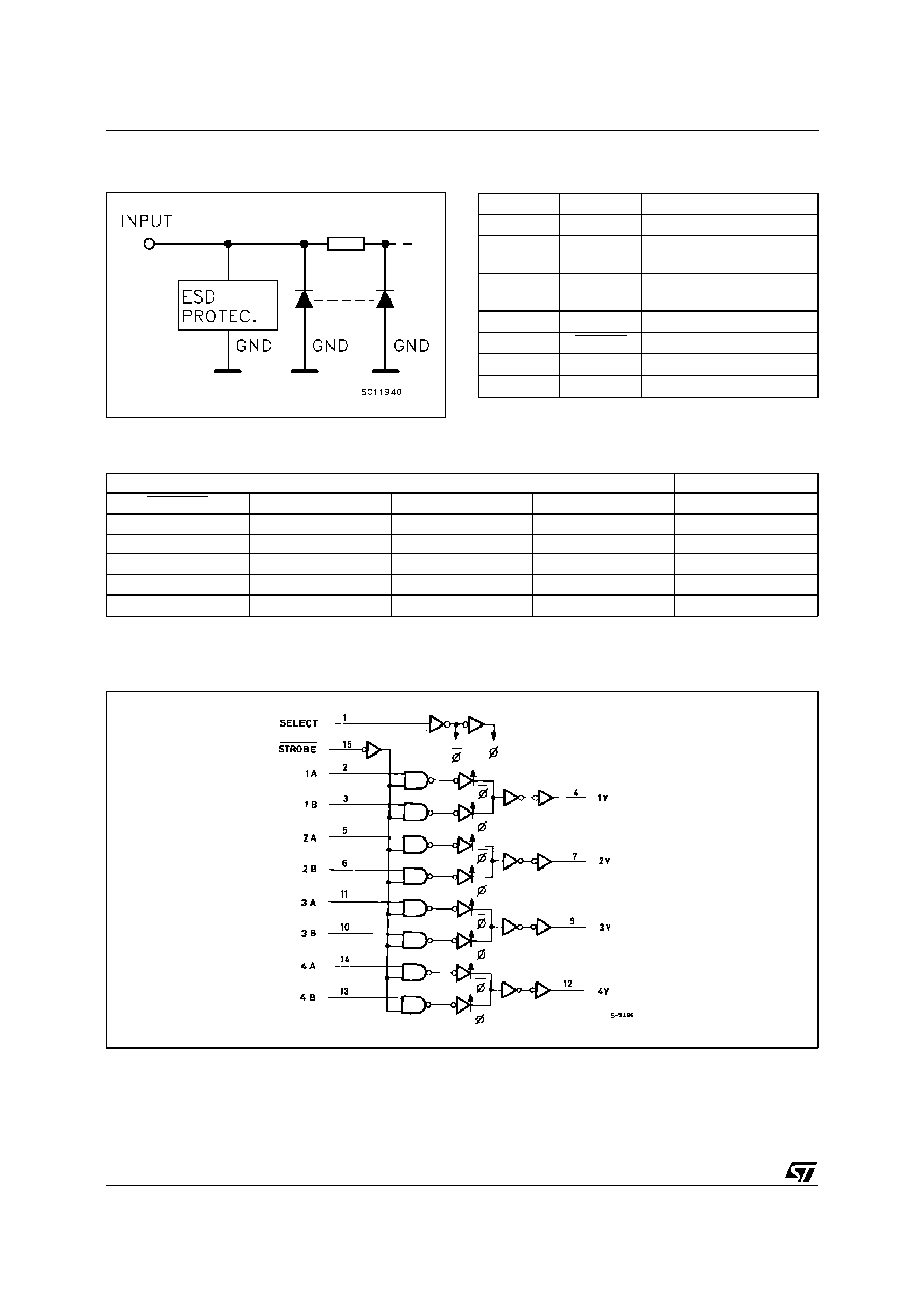
INPUT EQUIVALENT CIRCUIT
TRUTH TABLE
INPUT
OUT PUT
STROBE
SELE CT
A
B
Y
H
X
X
X
L
L
L
L
X
L
L
L
H
X
H
L
H
X
L
L
L
H
X
H
H
X:"H" or "L"
PIN DESCRIPTION
PIN No
SYMBOL
NAME AND FUNCT ION
1
SELECT
Common Data Select Input
2, 5, 11, 14
1A to 4A
Data Inputs From
Source A
3, 6, 10, 13
1B to 4B
Data Inputs From
Source B
4, 7,9, 12
1Y to 4Y
Multiplexer Outputs
15
STROBE
Strobe Input
8
GND
Ground (0V)
16
V
CC
Positive Supply Voltage
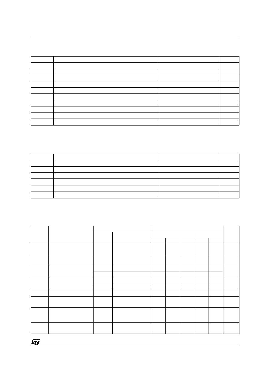
LOGIC DIAGRAM
74VHCT157A
2/9
RECOMMENDED OPERATING CONDITIONS
Symbol
Parameter
Valu e
Uni t
V
CC
Supply Voltage
4.5 to 5.5
V
V
I
Input Voltage
0 to 5.5
V
V
O
Output Voltage (see note 1)
0 to 5.5
V
V
O
Output Voltage (see note 2)
0 to V
CC
V
T
op
Operating Temperature
-40 to +85
o
C
dt/dv
Input Rise and Fall Time (see note 3) (V
CC
= 5.0
±
0.5V)
0 to 20
ns/V
1) V
CC
=0
2) High or Low State
3)V
IN
from0.8V to 2 V
ABSOLUTE MAXIMUM RATINGS
Symbol
Parameter
Val ue
Unit
V
CC
Supply Voltage
-0.5 to +7.0
V
V
I
DC Input Voltage
-0.5 to +7.0
V
V
O
DC Output Voltage (see note 1)
-0.5 to +7.0
V
V
O
DC Output Voltage (see note 2)
-0.5 to V
CC
+ 0.5
V
I
IK
DC Input Diode Current
- 20
mA
I
OK
DC Output Diode Current
±
20
mA
I
O
DC Output Current
±
25
mA
I
CC
orI
GND
DC V
CC
or Ground Current
±
50
mA
T
stg
Storage Temperature
-65 to +150
o
C
T
L
Lead Temperature (10 sec)
300
o
C
Absolute Maximum Ratings are those values beyond which damage to the device may occur. Functional operation under these condition is not implied.
1) V
CC
=0
2) High or Low State
DC SPECIFICATIONS
Symb ol
Parameter
T est Cond ition s
Val ue
Un it
V
CC
(V)
T
A
= 25
o
C
-40 to 85
o
C
Min.
Typ .
Max.
Min .
Max.
V
IH
High Level Input
Voltage
4.5 to 5.5
2
2
V
V
IL
Low Level Input
Voltage
4.5 to 5.5
0.8
0.8
V
V
OH
High Level Output
Voltage
4.5
I
O
=-50
µ
A
4.4
4.5
4.4
V
4.5
I
O
=-8 mA
3.94
3.8
V
OL
Low Level Output
Voltage
4.5
I
O
=50
µ
A
0.0
0.1
0.1
V
4.5
I
O
=8 mA
0.36
0.44
I
I
Input Leakage Current
0 to 5.5
V
I
= 5.5V or GND
±
0.1
±
1.0
µ
A
I
CC
Quiescent Supply
Current
5.5
V
I
= V
CC
orGND
4
40
µ
A
I
CC
Additional Worst Case
Supply Current
5.5
One Input at 3.4V,
other input at V
CC
or
GND
1.35
1.5
mA
I
OPD
Output Leakage
Current
0
V
OUT
= 5.5V
0.5
5.0
µ
A
74VHCT157A
3/9
CAPACITIVE CHARACTERISTICS
Symb ol
Parameter
T est Cond ition s
Val ue
Un it
T
A
= 25
o
C
-40 to 85
o
C
Min.
Typ .
Max.
Min .
Max.
C
IN
Input Capacitance
4
10
10
pF
C
PD
Power Dissipation
Capacitance (note 1)
20
pF
1) C
PD
isdefined as the value of the IC'sinternal equivalent capacitance which is calculated fromthe operating current consumption without load. (Referto
Test Circuit).Average operating current can be obtained by the following equation. I
CC
(opr) = C
PD
∑
V
CC
∑
f
IN
+ I
CC
/4 (per Channel)
AC ELECTRICAL CHARACTERISTICS (Input t
r
= t
f
=3 ns)
Symb ol
Parameter
Test Co nditi on
Val ue
Un it
V
CC
(V)
C
L
(pF )
T
A
= 25
o
C
-40 to 85
o
C
Min.
Typ .
Max.
Min .
Max.
t
PLH
t
PHL
Propagation Delay
Time
A, B to Y
5.0
(*)
15
6.2
9.7
1.0
11.5
ns
5.0
(*)
50
8.7
13.2
1.0
15.0
t
PLH
t
PHL
Propagation Delay
Time
SELECT to Y
5.0
(*)
15
8.4
13.2
1.0
15.5
ns
5.0
(*)
50
10.9
16.7
1.0
19.0
t
PLH
t
PHL
Propagation Delay
Time
STROBE to Y
5.0
(*)
15
8.7
13.6
1.0
16.0
ns
5.0
(*)
50
11.2
17.1
1.0
19.5
(*) Voltage range is 5V
±
0.5V
74VHCT157A
4/9
DYNAMIC SWITCHING CHARACTERISTICS
Symb ol
Parameter
T est Cond ition s
Val ue
Un it
V
CC
(V)
T
A
= 25
o
C
-40 to 85
o
C
Min.
Typ .
Max.
Min .
Max.
V
OLP
Dynamic Low Voltage
Quiet Output (note 1, 2)
5.0
C
L
= 50 pF
0.3
0.8
V
V
OLV
-0.8
-0.3
V
IHD
Dynamic High Voltage
Input (note 1, 3)
5.0
2.0
V
ILD
Dynamic Low Voltage
Input (note 1, 3)
5.0
0.8
1) Worst case package.
2) Max number of outputs defined as (n). Data inputs are driven 0V to 5.0V, (n -1) outputs switching and one output at GND.
3) Max number of data inputs (n) switching. (n-1) switching 0V to5.0V. Inputs under test switching: 5.0V to threshold (V
ILD
), 0V to threshold (V
IHD
), f=1MHz.
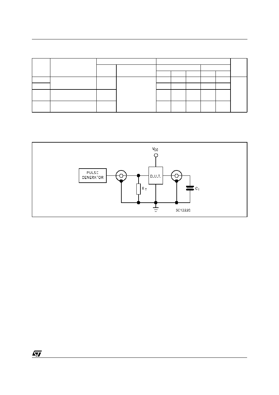
TEST CIRCUIT
C
L
= 15/50 pF or equivalent (includes jig and probe capacitance)
R
T
= Z
OUT
of pulse generator (typically 50
)
74VHCT157A
5/9