 | –≠–ª–µ–∫—Ç—Ä–æ–Ω–Ω—ã–π –∫–æ–º–ø–æ–Ω–µ–Ω—Ç: 79XX | –°–∫–∞—á–∞—Ç—å:  PDF PDF  ZIP ZIP |
1/16
February 2003
s
OUTPUT CURRENT UP TO 1.5A
s
OUTPUT VOLTAGES OF -5; -5.2; -6; -8; -9;
-12; -15; -18; -20; -22; -24V
s
THERMAL OVERLOAD PROTECTION
s
SHORT CIRCUIT PROTECTION
s
OUTPUT TRANSITION SOA PROTECTION
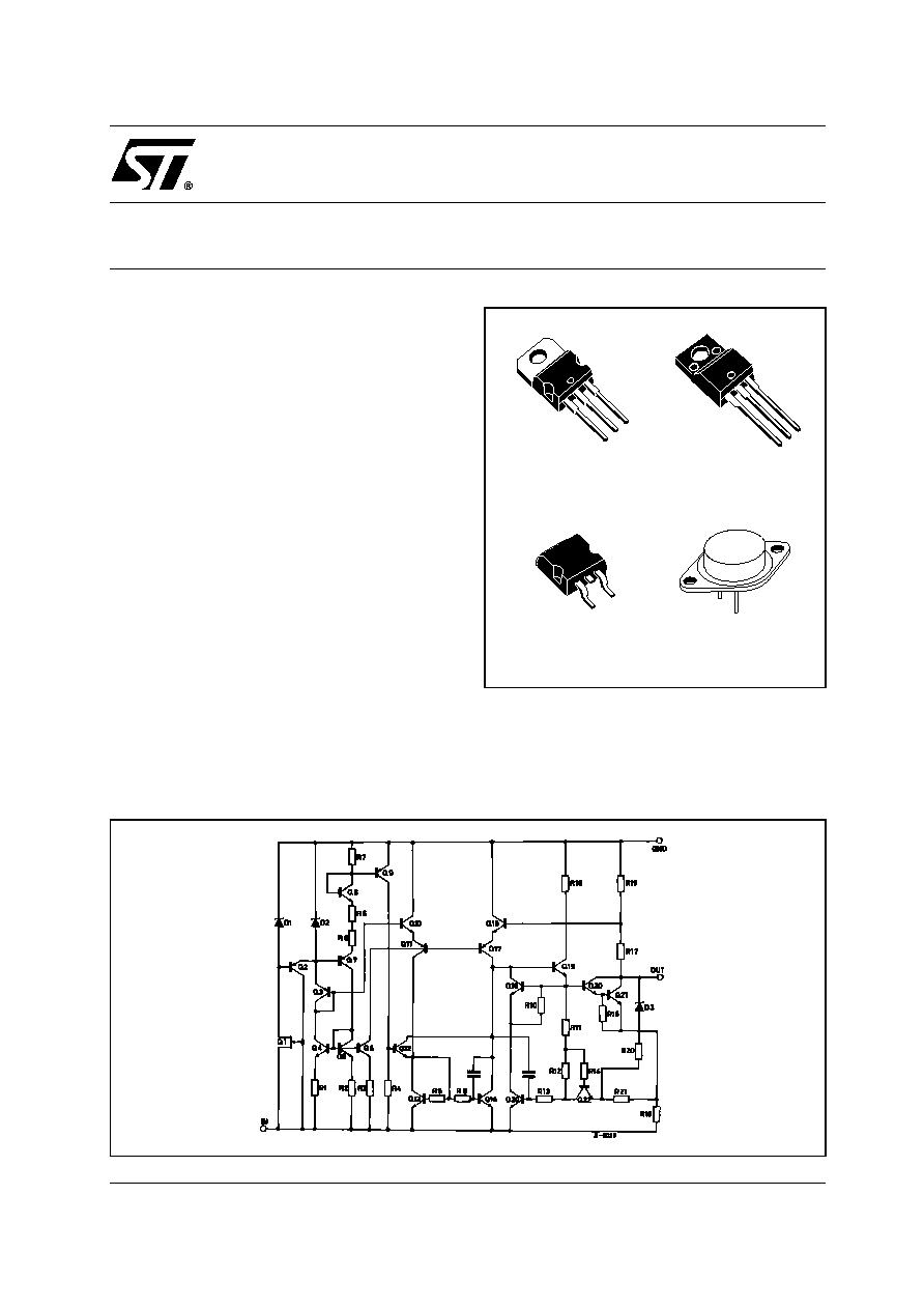
DESCRIPTION
The L7900 series of three-terminal negative
regulators is available in TO-220, TO-220FP,
TO-3 and D
2
PAK packages and several fixed
output voltages, making it useful in a wide range of
applications. These regulators can provide local
on-card regulation, eliminating the distribution
problems associated with single point regulation;
furthermore, having the same voltage option as
the L7800 positive standard series, they are
particularly suited for split power supplies. In
addition, the -5.2V is also available for ECL
system. If adequate heat sinking is provided, they
can deliver over 1.5A output current.
Although designed primarily as fixed voltage
regulators, these devices can be used with
external components to obtain adjustable voltages
and currents.
L7900
SERIES
NEGATIVE VOLTAGE REGULATORS
SCHEMATIC DIAGRAM
TO-220
D
2
PAK
TO-220FP
TO-3
L7900 SERIES
2/16
ABSOLUTE MAXIMUM RATINGS
Absolute Maximum Ratings are those values beyond which damage to the device may occur. Functional operation under these condition is
not implied.
THERMAL DATA
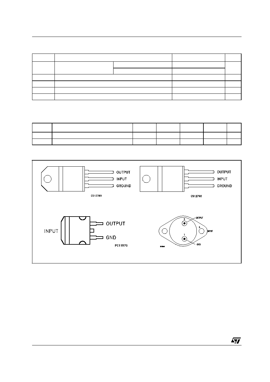
CONNECTION DIAGRAM (top view)
Symbol
Parameter≤
Value
Unit
V
I
DC Input Voltage
for V
O
= 5 to 18V
-35
V
for V
O
= 20, 24V
-40
I
O
Output Current
Internally Limited
P
tot
Power Dissipation
Internally Limited
T
stg
Storage Temperature Range
-65 to 150
∞C
T
op
Operating Junction Temperature Range
0 to 150
∞C
Symbol
Parameter
D
2
PAK
TO-220
TO-220FP
TO-3
Unit
R
thj-case
Thermal Resistance Junction-case
Max
3
3
5
4
∞C/W
R
thj-amb
Thermal Resistance Junction-ambient
Max
62.5
50
60
35
∞C/W
TO-220
TO-220FP
TO-3
D
2
PAK

L7900 SERIES
3/16
ORDERING CODES
(*) Available in Tape & Reel with the suffix "-TR".
TEST CIRCUIT
ELECTRICAL CHARACTERISTICS OF L7905C (refer to the test circuits, T
J
= 0 to 125∞C, V
I
= -10V,
I
O
= 500 mA, C
I
= 2.2 µF, C
O
= 1 µF unless otherwise specified).
(*) Load and line regulation are specified at constant junction temperature. Changes in V
O
due to heating effects must be taken into account
separately. Pulse testing with low duty cycle is used.
TYPE
TO-220
D
2
PAK (*)
TO-220FP
TO-3
OUTPUT VOLTAGE
L7905C
L7905CV
L7905ACD2T
L7905CP
L7905CT
-5 V
L7952C
L7952CV
L7952ACD2T
L7952CT
-5.2 V
L7906C
L7906CV
L7906ACD2T
L7906CP
L7906CT
-6 V
L7908C
L7908CV
L7908ACD2T
L7908CP
L7908CT
-8 V
L7912C
L7912CV
L7912ACD2T
L7912CP
L7912CT
-12 V
L7915C
L7915CV
L7915ACD2T
L7915CP
L7915CT
-15 V
L7918C
L7918CV
L7918ACD2T
L7918CP
L7918CT
-18 V
L7920C
L7920CV
L7920ACD2T
L7920CP
L7920CT
-20 V
L7922C
L7922CV
L7922ACD2T
L7922CT
-22 V
L7924C
L7924CV
L7924ACD2T
L7924CP
L7924CT
-24 V
Symbol
Parameter
Test Conditions
Min.
Typ.
Max.
Unit
V
O
Output Voltage
T
J
= 25∞C
-4.8
-5
-5.2
V
V
O
Output Voltage
I
O
= -5 mA to -1 A
P
O
15 W
V
I
= 8 to 20 V
-4.75
-5
-5.25
V
V
O
(*)
Line Regulation
V
I
= -7 to -25 V
T
J
= 25∞C
100
mV
V
I
= -8 to -12 V
T
J
= 25∞C
50
V
O
(*)
Load Regulation
I
O
= 5 mA to 1.5 A
T
J
= 25∞C
100
mV
I
O
= 250 to 750 mA
T
J
= 25∞C
50
I
d
Quiescent Current
T
J
= 25∞C
3
mA
I
d
Quiescent Current Change
I
O
= 5 mA to 1 A
0.5
mA
V
I
= -8 to -25 V
1.3
V
O
/
T Output Voltage Drift
I
O
= 5 mA
-0.4
mV/∞C
eN
Output Noise Voltage
B = 10Hz to 100KHz
T
J
= 25∞C
100
µ
V
SVR
Supply Voltage Rejection
V
I
= 10 V
f = 120Hz
54
60
dB
V
d
Dropout Voltage
I
O
= 1 A
T
J
= 25∞C
V
O
= 100 mV
1.4
V
I
sc
Short Circuit Current
2.1
A
L7900 SERIES
4/16
ELECTRICAL CHARACTERISTICS OF L7952C (refer to the test circuits, T
J
= 0 to 125∞C, V
I
= -10V,
I
O
= 500 mA, C
I
= 2.2 µF, C
O
= 1 µF unless otherwise specified).
(*) Load and line regulation are specified at constant junction temperature. Changes in V
O
due to heating effects must be taken into account
separately. Pulse testing with low duty cycle is used.
ELECTRICAL CHARACTERISTICS OF L7906C (refer to the test circuits, T
J
= 0 to 125∞C, V
I
= -11V,
I
O
= 500 mA, C
I
= 2.2 µF, C
O
= 1 µF unless otherwise specified).
(*) Load and line regulation are specified at constant junction temperature. Changes in V
O
due to heating effects must be taken into account
separately. Pulse testing with low duty cycle is used.
Symbol
Parameter
Test Conditions
Min.
Typ.
Max.
Unit
V
O
Output Voltage
T
J
= 25∞C
-5.0
-5.2
-5.4
V
V
O
Output Voltage
I
O
= -5 mA to -1 A
P
O
15 W
V
I
= -9 to -21 V
-4.95
-5.2
-5.45
V
V
O
(*)
Line Regulation
V
I
= -8 to -25 V
T
J
= 25∞C
105
mV
V
I
= -9 to -12 V
T
J
= 25∞C
52
V
O
(*)
Load Regulation
I
O
= 5 mA to 1.5 A
T
J
= 25∞C
105
mV
I
O
= 250 to 750 mA
T
J
= 25∞C
52
I
d
Quiescent Current
T
J
= 25∞C
3
mA
I
d
Quiescent Current Change
I
O
= 5 mA to 1 A
0.5
mA
V
I
= -9 to -25 V
1.3
V
O
/
T Output Voltage Drift
I
O
= 5 mA
-0.5
mV/∞C
eN
Output Noise Voltage
B = 10Hz to 100KHz
T
J
= 25∞C
125
µ
V
SVR
Supply Voltage Rejection
V
I
= 10 V
f = 120Hz
54
60
dB
V
d
Dropout Voltage
I
O
= 1 A
T
J
= 25∞C
V
O
= 100 mV
1.4
V
I
sc
Short Circuit Current
2
A
Symbol
Parameter
Test Conditions
Min.
Typ.
Max.
Unit
V
O
Output Voltage
T
J
= 25∞C
-5.75
-6
-6.25
V
V
O
Output Voltage
I
O
= -5 mA to -1 A
P
O
15 W
V
I
= -9.5 to -21.5 V
-5.7
-6
-6.3
V
V
O
(*)
Line Regulation
V
I
= -8.5 to -25 V
T
J
= 25∞C
120
mV
V
I
= -9 to -15 V
T
J
= 25∞C
60
V
O
(*)
Load Regulation
I
O
= 5 mA to 1.5 A
T
J
= 25∞C
120
mV
I
O
= 250 to 750 mA
T
J
= 25∞C
60
I
d
Quiescent Current
T
J
= 25∞C
3
mA
I
d
Quiescent Current Change
I
O
= 5 mA to 1 A
0.5
mA
V
I
= -9.5 to -25 V
1.3
V
O
/
T Output Voltage Drift
I
O
= 5 mA
-0.6
mV/∞C
eN
Output Noise Voltage
B = 10Hz to 100KHz
T
J
= 25∞C
144
µ
V
SVR
Supply Voltage Rejection
V
I
= 10 V
f = 120Hz
54
60
dB
V
d
Dropout Voltage
I
O
= 1 A
T
J
= 25∞C
V
O
= 100 mV
1.4
V
I
sc
Short Circuit Current
2
A

L7900 SERIES
5/16
ELECTRICAL CHARACTERISTICS OF L7908C (refer to the test circuits, T
J
= 0 to 125∞C, V
I
= -14V,
I
O
= 500 mA, C
I
= 2.2 µF, C
O
= 1 µF unless otherwise specified).
(*) Load and line regulation are specified at constant junction temperature. Changes in V
O
due to heating effects must be taken into account
separately. Pulse testing with low duty cycle is used.
ELECTRICAL CHARACTERISTICS OF L7912C (refer to the test circuits, T
J
= 0 to 125∞C, V
I
= -19V,
I
O
= 500 mA, C
I
= 2.2 µF, C
O
= 1 µF unless otherwise specified).
(*) Load and line regulation are specified at constant junction temperature. Changes in V
O
due to heating effects must be taken into account
separately. Pulse testing with low duty cycle is used.
Symbol
Parameter
Test Conditions
Min.
Typ.
Max.
Unit
V
O
Output Voltage
T
J
= 25∞C
-7.7
-8
-8.3
V
V
O
Output Voltage
I
O
= -5 mA to -1 A
P
O
15 W
V
I
= -11.5 to -23 V
-7.6
-8
-8.4
V
V
O
(*)
Line Regulation
V
I
= -10.5 to -25 V
T
J
= 25∞C
160
mV
V
I
= -11 to -17 V
T
J
= 25∞C
80
V
O
(*)
Load Regulation
I
O
= 5 mA to 1.5 A
T
J
= 25∞C
160
mV
I
O
= 250 to 750 mA
T
J
= 25∞C
80
I
d
Quiescent Current
T
J
= 25∞C
3
mA
I
d
Quiescent Current Change
I
O
= 5 mA to 1 A
0.5
mA
V
I
= -11.5 to -25 V
1
V
O
/
T Output Voltage Drift
I
O
= 5 mA
-0.6
mV/∞C
eN
Output Noise Voltage
B = 10Hz to 100KHz
T
J
= 25∞C
175
µ
V
SVR
Supply Voltage Rejection
V
I
= 10 V
f = 120Hz
54
60
dB
V
d
Dropout Voltage
I
O
= 1 A
T
J
= 25∞C
V
O
= 100 mV
1.1
V
I
sc
Short Circuit Current
1.5
A
Symbol
Parameter
Test Conditions
Min.
Typ.
Max.
Unit
V
O
Output Voltage
T
J
= 25∞C
-11.5
-12
-12.5
V
V
O
Output Voltage
I
O
= -5 mA to -1 A
P
O
15 W
V
I
= -15.5 to -27 V
-11.4
-12
-12.6
V
V
O
(*)
Line Regulation
V
I
= -14.5 to -30 V
T
J
= 25∞C
240
mV
V
I
= -16 to -22 V
T
J
= 25∞C
120
V
O
(*)
Load Regulation
I
O
= 5 mA to 1.5 A
T
J
= 25∞C
240
mV
I
O
= 250 to 750 mA
T
J
= 25∞C
120
I
d
Quiescent Current
T
J
= 25∞C
3
mA
I
d
Quiescent Current Change
I
O
= 5 mA to 1 A
0.5
mA
V
I
= -15 to -30 V
1
V
O
/
T Output Voltage Drift
I
O
= 5 mA
-0.8
mV/∞C
eN
Output Noise Voltage
B = 10Hz to 100KHz
T
J
= 25∞C
200
µ
V
SVR
Supply Voltage Rejection
V
I
= 10 V
f = 120Hz
54
60
dB
V
d
Dropout Voltage
I
O
= 1 A
T
J
= 25∞C
V
O
= 100 mV
1.1
V
I
sc
Short Circuit Current
1.5
A