 | –≠–ª–µ–∫—Ç—Ä–æ–Ω–Ω—ã–π –∫–æ–º–ø–æ–Ω–µ–Ω—Ç: 8169 | –°–∫–∞—á–∞—Ç—å:  PDF PDF  ZIP ZIP |
1/30
STA304A
March 2002
This is preliminary information on a new product foreseen to be developed. Details are subject to change without notice.
s
STA304AEND TO END DIGITAL AUDIO
INTEGRATED SOLUTION
s
∑ DSP Functions:
- DIGITAL VOLUME CONTROL
- SOFT MUTE
- BASS and TREBLE
- PARAMETRIC EQ PER CHANNEL
- BASS MANAGEMENT FOR SUBWOOFER
- AUTO MUTE ON ZERO INPUT DETECTION
s
4+1 DIRECT DIGITAL AMPLIFICATION
(DDXTM) OUTPUT CHANNELs
s
6 CHANNELs PROGRAMMABLE SERIAL
OUTPUT INTERFACE (by default I2S)
s
4 CHANNELs PROGRAMMABLE SERIAL
INPUT INTERFACE (by default I2S)
s
STEREO S/PDIF INPUT INTERFACE
s
Intel AC'97 LINK (rev. 2.1) INPUT INTERFACE
FOR AUDIO AND CONTROL
s
ON CHIP AUTOMATIC INPUT SAMPLING
FREQUENCY DETECTION
s
100 dB SNR SAMPLE RATE CONVERTER
(1KHz SINUSOIDAL INPUT)
s
I
2
C CONTROL BUS
s
LOW POWER 3.3V CMOS TECHNOLOGY
s
EMBEDDED PLL FOR INTERNAL CLOCK
GENERATION (1024x48 kHz = 49.152 MHz)
s
6.144 MHz EXTERNAL INPUT CLOCK OR
BUILT-IN INDUSTRY STANDARD XTAL
OSCILLATOR
s
VARIABLE DIGITAL GAIN UP TO 24dB
(0.75dB STEP)
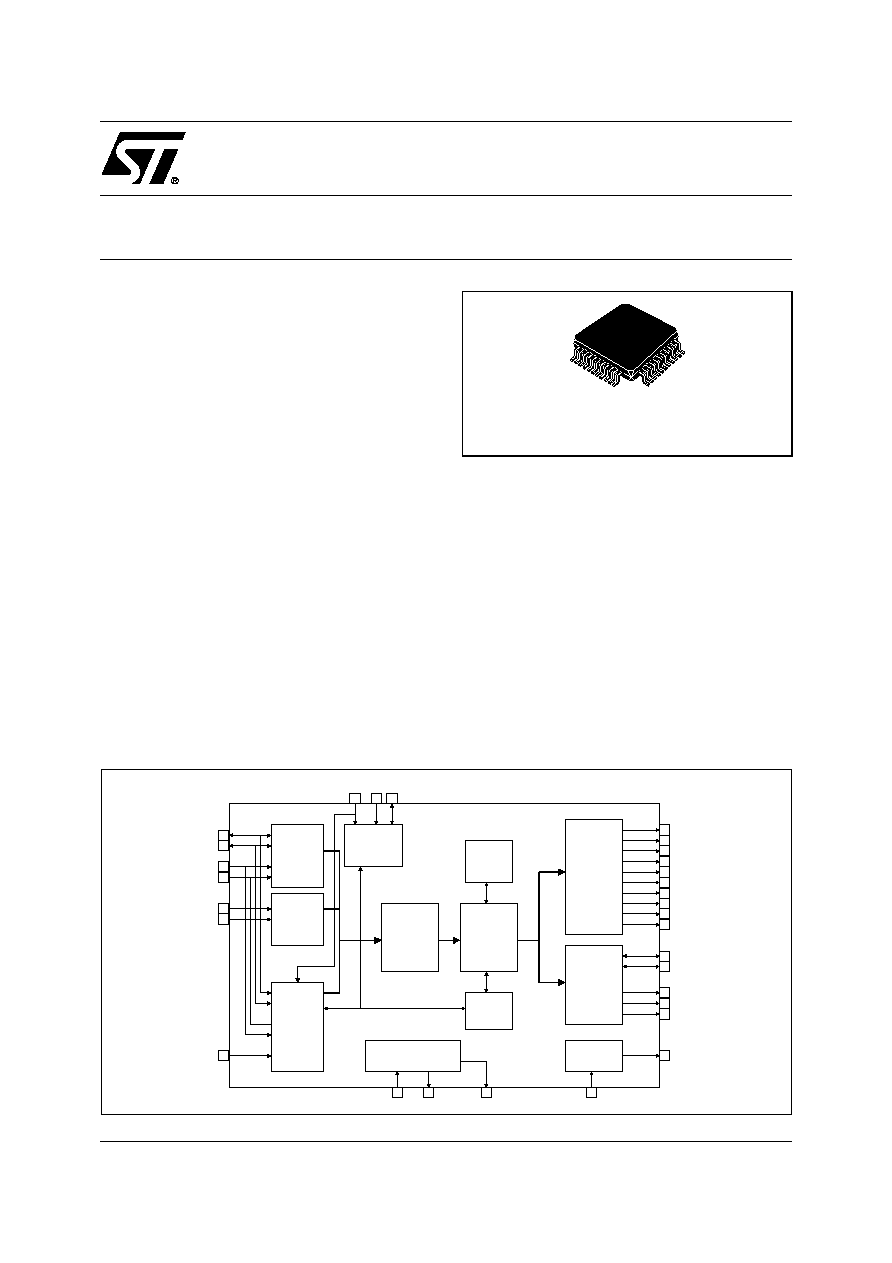
1.0 DESCRIPTION
The STA304A Digital Audio Processor is a single
chip device implementing end to end digital solution
for audio application. In conjunction with STA500
power bridge it gives the full digital DSP-to-power
high quality chain with no need for audio Digital-to-
Analog converters between DSP and power stage.
TQFP44
ORDERING NUMBER: STA304A
PRODUCT PREVIEW
DIGITAL AUDIO PROCESSOR WITH MULTICHANNEL DDXTM
BLOCK DIAGRAM
DSP
SRC
I2S
AC`97
S/PDIF
DDX
I2S
PLL
I2C
RESET
LRCKI / SYNC
SDI_1 / SDATA_OUT
SDI_2 / SDATA_IN
RXP
RXN
BICKI / BIT_CL
SDO_1
SDO_2
SDO_3
LRCKO
BICKO
XTI
XTO
LEFT_A
LEFT_B
RIGHT_A
RIGHT_B
SLEFT_A
SLEFT_B
SRIGHT_A
SRIGHT_B
LFE_A
LFE_B
SCL
SDA
SA
RAM
ROM
CKOUT
18
1
2
3
4
19
11
10
9
7
14
15
43
43
43
43
43
43
22
21
24
23
34
33
28
27
30
29
PowerDown
44
35
EAPD
PWDN
STA304A
2/30
1.0 DESCRIPTION (continued)
The device supports two main configurations as far as input sources: AC'97 input or IIS/SPDIF input: selection
is made via a dedicated pin (
AC97_MODE
pin). The AC`97 can be configured to work in two different ways:
'Full Compliant' mode and 'Proprietary' mode which enables more features. The selection of the operating mode
is done via a specific bit in a Vendor Reserved register (see bit 0: AC97_FC_mode in the CRA register, address
5Ah).
The 'Full Compliant' mode is compliant with rev. 2.1 of AC`97 link specifications.
This link can provide up to 6 input audio channels with sampling frequency of 44.1, 48, 88.2, 96 kHz, and the
related controls.
In the IIS/SPDIF mode, a stereo S/PDIF and a 4 channels three-wires programmable serial input interface work
in mutually exclusive way. Two channels with sampling frequency in the continuous range from 32 to 96 kHz
are supported by the S/PDIF interface. Up to four channels with sampling frequency varying continuously from
32kHz up to 96 kHz are supported by the programmable serial interfaces. Among the different configurations,
also the standard IIS protocol is supported.
An embedded high quality sample rate converter (SRC) resamples input data at the internal fixed sampling fre-
quency of 48 kHz for DSP operations.
The DSP is a 20x20 bit core audio processor performing several user controlled parametric algorithms, among
them are dynamic and static equalization, Bass, Treble, Volume control and more. The DSP operates at
49.152MHz (1024xfs). This frequency is generated by an internal PLL with programmable multiplication factor
(x2 or x8).
This device has 5 channels Direct Digital Amplification (DDXTM technology), performing high efficiency class-D
PWM output signals used to drive directly external power bridge stages (STA500).
In addition a 6 channel digital output programmable interface (supporting IIS standard protocol) is embedded
for applications with commercial audio D/A converters. The output sampling frequency is fixed at 48 kHz when
the interface operates as master. In addition an oversampled clock (256xfs or 512xfs) is provided externally for
the D/A converters.
An IIC interface allows full programmability of internal algorithms and control registers via an external controller.
An arbitration logic handles access conflicts to embedded control registers (which may occur as a consequence
of contemporary access to control registers by AClink, IIC and DSP blocks).
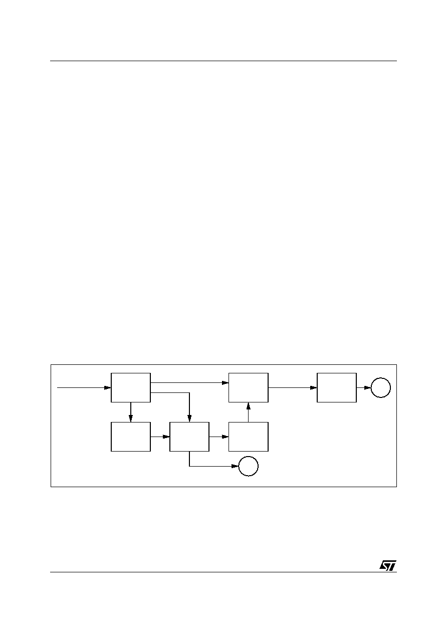
Figure 1. DSP data processing
BASS
REDIR
STATIC &
DINAMIC
EQ
VOLUME
CENTER
VOLUME
PHANTOM
CENTER
BASS
TREBLE
I2S
SL/SR/LFE
CNT
CNT
L/R
L/R
L/R
L,R,SL,SR,LFE,CNT
L,R,SL,SR,LFE
I2S +
DDX
D01AU1310
3/30
STA304A
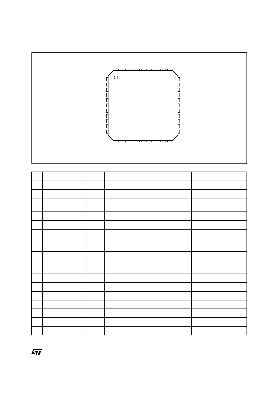
PIN CONNECTION (Top view)
PIN FUNCTION
PIN
NAME
TYPE
DESCRIPTION
PAD TYPE
1
SDI_1 / SDATA_OUT
I
Input I2S Serial Data 1 / AC97 Output Data
CMOS Schmitt In
2
SDI_2 / SDATA_IN
I/O
Input I2S Serial Data 2 / AC97 Input Data
CMOS In / CMOS Out 2mA
3
LRCKI / SYNC
I/O
Input I2S Left/Right Clock / AC97 Synch.
Clock
CMOS In / CMOS Out 2mA
4
BICKI / BIT_CLK
I/O
Input I2S Serial Clock / AC97 Bit Clock
CMOS In / CMOS Out 4mA
5
VDD_1
Digital Supply Voltage
6
GND_1
Digital Ground
7
RESET
I
Global Reset
(This pin is sensed only after 2 clock cycles)
CMOS Schmitt In Pull-Up
8
AC97_MODE
I
AC97 Enable / Disable (1=AC97; 0=I2S/
SPDIF)
CMOS Schmitt In Pull-Down
9
SDA
I/O
I2C Serial Data
CMOS In / CMOS Out 2mA
10
SCL
I
I2C Serial Clock
CMOS In
11
SA
Select Address (I2C / AC97)
CMOS In
12
TEST_MODE
I
Test Mode (Active High)
CMOS
13
VDD_2
Digital Supply Voltage
14
XTI
I
Crystal Input (Clock input)
Analog IN
15
XTO
O
Crystal Output
CMOS Out Oscill. Pad
16
GND_2
Digital Ground
1
2
3
5
6
4
7
8
9
10
17
11
18
19
20
21
22
44
43
42
41
39
40
38
37
36
35
34
28
27
26
24
23
25
33
32
31
29
30
SDI_1/SDATA_OUT
SDI_2/SDATA_IN
LRCKI/SYNC
BICKI/BIT_CLK
VDD_1
GND_1
RESET
AC97_MODE
SDA
SCL
SA
TEST_MODE
VDD_2
XTI
XTO
GND_2
VCC
RXP
RXN
VSS
LFE_B
LFE_A
SLEFT_A
EAPD
LRCKO
SDO_1
SDO_2
SDO_3
SCKO
GND_5
VDD_5
CKOUT
PWDN
SRIGHT_B
SRIGHT_A
GND_3
VDD_3
RIGHT_B
RIGHT_A
LEFT_B
LEFT_A
GND_4
VDD_4
SLEFT_B
D00AU1160
12
13
14
15
16
STA304A
4/30
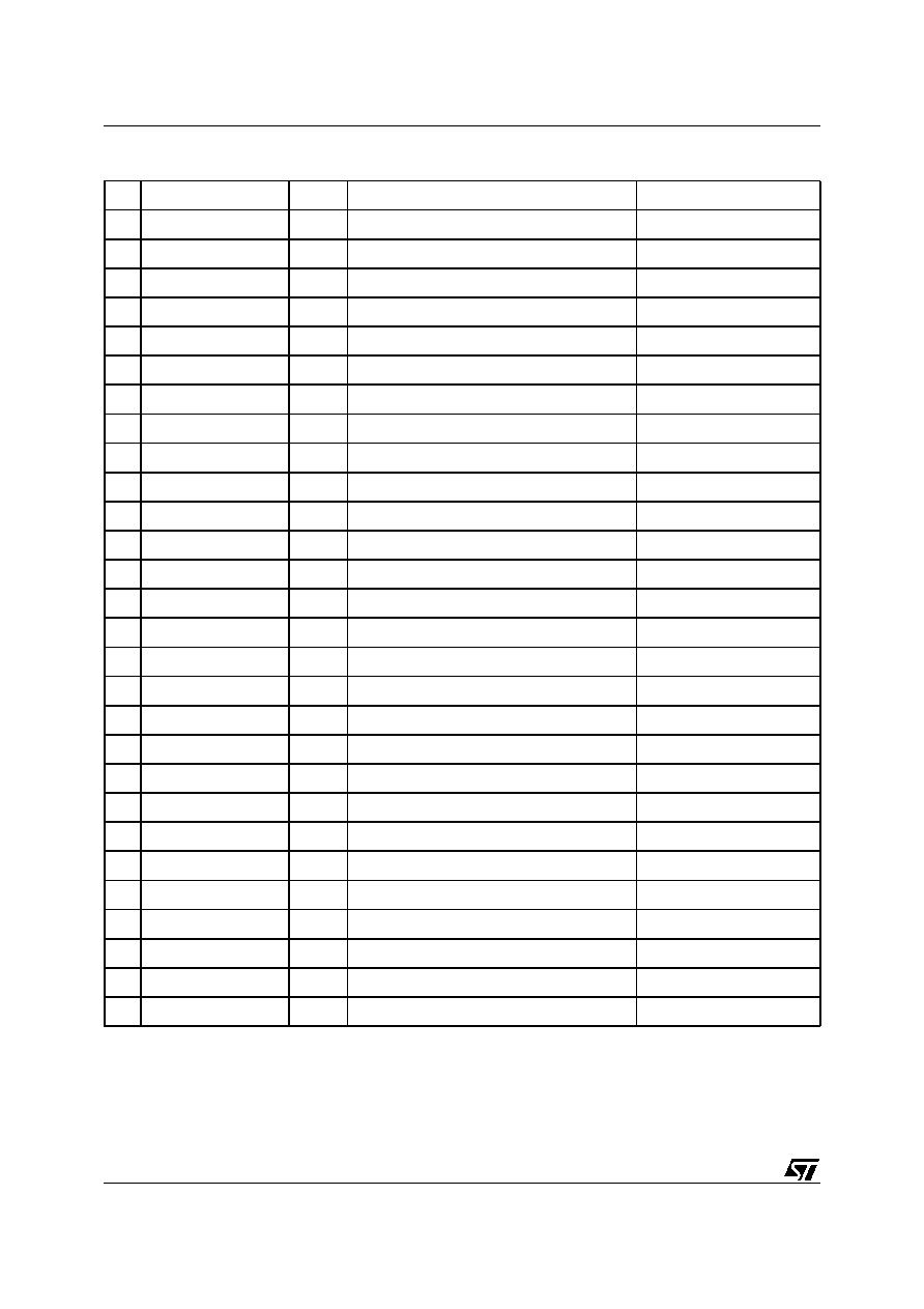
PIN
NAME
TYPE
DESCRIPTION
PAD TYPE
17
VCC
Analog Supply Voltage
18
RXP
I
S/PDIF receiver positive
Analog In
19
RXN
I
S/PDIF receiver negative
Analog In
20
VSS
Analog Ground
21
LFE_B
O
Pwm LFE (subwoofer) output channel (B)
CMOS Out 3mA
22
LFE_A
O
Pwm LFE (subwoofer) output channel (A)
CMOS Out 3mA
23
SRIGHT_B
O
Pwm Surround Right output channel (B)
CMOS Out 3mA
24
SRIGHT_A
O
Pwm Surround Right output channel (A)
CMOS Out 3mA
25
GND_3
Digital Ground
26
VDD_3
Digital Supply Voltage
27
RIGHT_B
O
Pwm Right output channel (B)
CMOS Out 3mA
28
RIGHT_A
O
Pwm Right output channel (A)
CMOS Out 3mA
29
LEFT_B
O
Pwm Left output channel (B)
CMOS Out 3mA
30
LEFT_A
O
Pwm Left output channel (A)
CMOS Out 3mA
31
GND_4
Digital Ground
32
VDD_4
Digital Supply Voltage
33
SLEFT_B
O
Pwm Surround Left output channel (B)
CMOS Out 3mA
34
SLEFT_A
O
Pwm Surround Left output channel (A)
CMOS Out 3mA
35
EAPD
O
External Amplifier Powerdown (Active Low)
CMOS Out 2mA
36
LRCKO
I/O
Output I2S Left/Right Clock
CMOS In / CMOS Out 2mA
37
SDO_1
O
Output I2S Serial Data 1
CMOS Out 2mA
38
SDO_2
O
Output I2S Serial Data 2
CMOS Out 2mA
39
SDO_3
O
Output I2S Serial Data 3
CMOS Out 2mA
40
SCKO
I/O
Output I2S Serial Clock
CMOS In / CMOS Out 4mA
41
GND_5
Digital Ground
42
VDD_5
Digital Supply Voltage
43
CKOUT
O
Clock Output (12 /24 MHz)
CMOS Out 8mA
44
PWDN
I
Device Powerdown (Active Low)
CMOS In Pull-Up
PIN FUNCTION (continued)
5/30
STA304A
ABSOLUTE MAXIMUM RATINGS
THERMAL DATA
ELECTRICAL CHARACTERISTCS (V
DD
= 3.3V ± 0.3V; T
amb
= 0 to 70 ∞C; unless otherwise specified)
DC OPERATING CONDITIONS
GENERAL INTERFACE ELECTRICAL CHARACTERISTICS
Note 1: The leakage currents are generally very small, < 1na. The value given here is a maximum that can occur after an electrostatic stress
on the pin.
Note 2: Human Body Model
Symbol
Parameter
Value
Unit
V
DD
Power Supply
-0.3 to 4
V
V
i
Voltage on input pins
-0.3 to VDD+0.3
V
V
o
Voltage on output pins
-0.3 to VDD+0.3
V
T
stg
Storage Temperature
-40 to +150
∞
C
T
op
Operative ambient temperature
-20 to +85
∞
C
P
DD
Power Consumption Digital
tbd
mW
P
DA
Power Consumption Analog
tbd
mW
Symbol
Parameter
Value
Unit
R
thj-amb
Thermal resistance Junction to Ambient
85
∞
C/W
Symbol
Parameter
Value
V
DD
Power Supply Voltage
3.0 to 3.6V
T
j
Operating Junction Temperature
-20 to 125
∞
C
Symbol
Parameter
Test Condition
Min.
Typ.
Max.
Unit
Note
I
il
Low Level Input Current Without
pull-up device
V
i
= 0V
-10
10
µ
A
1
I
ih
High Level Input Current
Without pull-up device
V
i
= V
DD
= 3.6V
-10
10
µ
A
1
V
esd
Electrostatic Protection
Leakage < 1
µ
A
2000
V
2