 | –≠–Ľ–Ķ–ļ—ā—Ä–ĺ–Ĺ–Ĺ—č–Ļ –ļ–ĺ–ľ–Ņ–ĺ–Ĺ–Ķ–Ĺ—ā: 8785 | –°–ļ–į—á–į—ā—Ć:  PDF PDF  ZIP ZIP |
1/13
January 2003
s
EDS PROTECTION FOR RS-232 I/O PINS:
Ī15KV HUMAN BODY MODEL
Ī8KV IEC 1000-4-2 CONTACT DISCHARGE
s
1
Ķ
A LOW POWER SHUTDOWN WITH
RECEIVERS ACTIVE
s
GUARENTEED DATA RATE
250Kbps (Normal Operation)
1Mbps (Very High Speed Operation)
s
GUARANTEED SLEW RATE RANGE
6V/
Ķ
s (Normal Operation)
24V/
Ķ
s (Very High Speed Operation)
s
0.1
Ķ
F EXTERNAL CAPACITORS
s
FLOW-THROUGH PINOUT
s
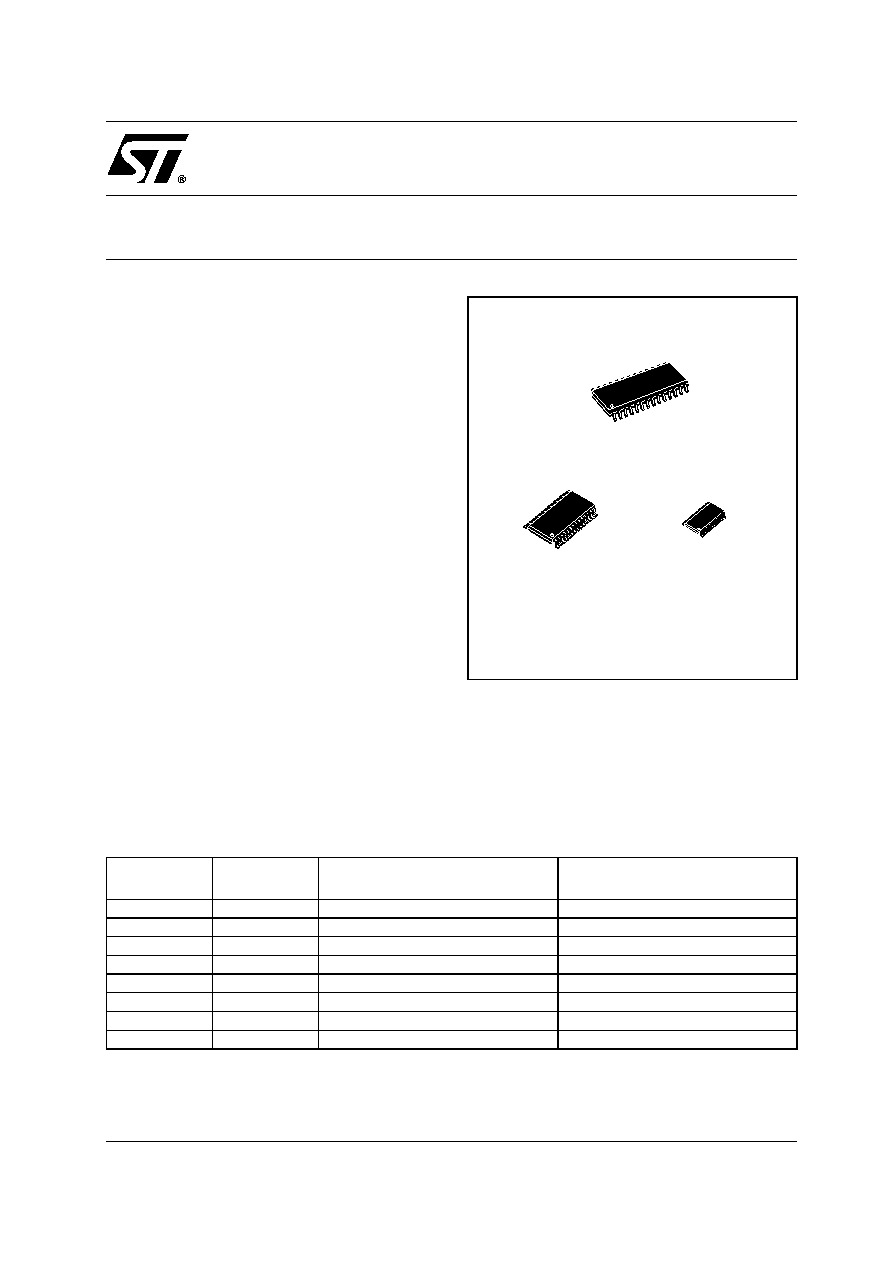
AVAILABLE IN SO-28, SSOP-28 AND
TSSOP28
s
LOW SUPPLY CURRENT 300
Ķ
A
DESCRIPTION
The ST3237E is a 3V to 5.5V powered EIA/
TIA-232 and V.28/V.24 communication interfaces
high
data-rate
capability
and
enhanced
electrostatic discharge (ESD) protection at Ī8KV
using IEC1000-4-2 contact discharge and Ī15kV
using Human Body Model (HBM). The other pins
are protected with standard ESD protection at
Ī2kV using HBM method. The ST3237C is a
transceiver (5 drivers, 3 receivers) for fast modem
applications.
The
device
has
a
proprietary
low-dropout
transmitter output stage providing true RS-232
performance from a 3V to 5.5V supply using a
dual charge pump. The device is guaranteed to
run at data rates of 250Kbps in the normal
operation mode and 1Mbps in the very high speed
operation mode while maintaining RS-232 output
levels.
ORDERING CODES
Type
Temperature
Range
Package
Comments
ST3237ECD
0 to 70 įC
SO-28 (Tube)
27parts per tube / 12tube per box
ST3237EBD
-40 to 85 įC
SO-28 (Tube)
27parts per tube / 12tube per box
ST3237ECDR
0 to 70 įC
SO-28 (Tape & Reel)
1000 parts per reel
ST3237EBDR
-40 to 85 įC
SO-28 (Tape & Reel)
1000 parts per reel
ST3237ECPR
0 to 70 įC
SSOP-28 (Tape & Reel)
1350 parts per reel
ST3237EBPR
-40 to 85 įC
SSOP-28 (Tape & Reel)
1350 parts per reel
ST3237ECTR (*)
0 to 70 įC
TSSOP28 (Tape & Reel)
2500 parts per reel
ST3237EBTR
-40 to 85 įC
TSSOP28 (Tape & Reel)
2500 parts per reel
ST3237E
Ī15KV ESD-PROTECTED, 1
Ķ
A, 3 TO 5.5V, 250KBPS,
RS-232 TRANSCEIVER WITH STAND-BY
SSOP
SOP
TSSOP
ST3237E
2/13
PIN DESCRIPTION
PlN Nį
SYMBOL
NAME AND FUNCTION
1
C
2
+
Positive Terminal of Inverting Charge Pump Capacitor
2
GND
Ground
3
C
2
-
Negative Terminal of Inverting Charge Pump Capacitor
4
V-
-5.5V Generated by the Charge Pump
5
T1
OUT
First Transmitter Output Voltage
6
T2
OUT
Second Transmitter Output Voltage
7
T3
OUT
Third Transmitter Output Voltage
8
R1
IN
First Receiver Input Voltage
9
R2
IN
Second Receiver Input Voltage
10
T4
OUT
Fourth Transmitter Output Voltage
11
R3
IN
Third Receiver Input Voltage
12
T5
OUT
Fifth Transmitter Output Voltage
13
EN
Receiver Enable, Active Low
14
SHDN
Shutdown Control, Active Low
15
VHSCI
Very High Speed Control Input. Connected to GND for normal
operation; connected to VCC for 1Mbps transmission rates.
16
R1
OUTB
Non Inverting Complementary Receiver Output. Always Active.
17
T5
IN
Fifth Transmitter Input Voltage
18
R3
OUT
Third Receiver Output Voltage
19
T4
IN
Fourth Transmitter Input Voltage
20
R2
OUT
Second Receiver Output Voltage
21
R1
OUT
First Receiver Output Voltage
22
T3
IN
Third Transmitter Input Voltage
23
T2
IN
Second Transmitter Input Voltage
24
T1
N
First Transmitter Input Voltage
25
C
1
-
Negative Terminal of Voltage-Doubler Charge Pump Capacitor
26
V
CC
Supply Voltage
27
V+
5.5V Generated by the Charge Pump
28
C
1
+
Positive Terminal of Voltage-Doubler Charge Pump Capacitor

ST3237E
3/13
PIN CONFIGURATION
ABSOLUTE MAXIMUM RATINGS
Absolute Maximum Ratings are those values beyond which damage to the device may occur. Functional operation under these condition is
not implied. V+ and V- can have a maximum magnitude of +7V, but their absolute addition can not exceed 13 V.
SHUTDOWN AND ENABLE CONTROL TRUTH TABLE
Symbol
Parameter
Value
Unit
V
CC
Supply Voltage
-0.3 to 6
V
V+
Doubled Voltage Terminal
-0.3 to 7
V
V-
Inverted Voltage Terminal
0.3 to -7
V
V+ +|V-|
13
V
T
IN
Transmitter Input Voltage Range
-0.3 to 6
V
SHDN, EN
-0.3 to 6
V
VHSCI
Very High Speed Control Input
-0.3 to (V
CC
+0.3)
V
R
IN
Receiver Input Voltage Range
Ī
25
V
T
OUT
Transmitter Output Voltage Range
Ī
13.2
V
R
OUT
, R
OUTB
Receiver Output Voltage Range
-0.3 to (V
CC
+ 0.3)
V
t
SHORT
Short Circuit Duration on T
OUT
(one at a time)
Continuous
T
stg
Storage Temperature Range
-65 to 150
įC
SHDN
EN
T-OUT
R-OUT
R-OUTB
0
0
High Z
Active
Active
0
1
High Z
High Z
Active
1
0
Active
Active
Active
1
1
Active
High Z
Active
ST3237E
4/13
ESD PERFORMANCE: TRANSMITTER OUTPUTS, RECEIVER INPUTS
ELECTRICAL CHARACTERISTICS
(C
1
- C
4
= 0.1
Ķ
F, V
CC
= 3V to 5.5V, T
A
= -40 to 85įC, unless otherwise specified.
Typical values are referred to T
A
= 25įC)
LOGIC INPUT ELECTRICAL CHARACTERISTICS
(C
1
- C
4
= 0.1
Ķ
F, V
CC
= 3V to 5.5V, T
A
= -40 to 85įC, unless otherwise specified.
Typical values are referred to T
A
= 25įC)
Note 1: Transmitter input hysteresis is typically 250mV
TRANSMITTER ELECTRICAL CHARACTERISTICS
(C
1
- C
4
= 0.1
Ķ
F tested at 3.3V
Ī
10%, V
CC
= 3V to 5.5V, T
A
= -40 to 85įC, unless otherwise specified.
Typical values are referred to T
A
= 25įC)
Symbol
Parameter
Test Conditions
Min.
Typ.
Max.
Unit
ESD
ESD Protection Voltage
Human Body Model
Ī
15
kV
ESD
ESD Protection Voltage
IEC-1000-4-2 Contact Discharge
Ī
8
kV
Symbol
Parameter
Test Conditions
Min.
Typ.
Max.
Unit
I
SUPPLY
V
CC
Power Supply Current
SHDN=V
CC
No Load
0.3
1
mA
I
SHDN
Shutdown Supply Current
SHDN=GND V
T_IN
=GND or V
CC
1
5
Ķ
A
Symbol
Parameter
Test Conditions
Min.
Typ.
Max.
Unit
V
TIL
Input Logic Threshold Low
(Note 1)
T-IN, VHSCI, EN, SHDN
0.8
V
V
TIH
Input Logic Threshold High
T-IN, VHSCI, EN, SHDN
V
CC
= 3.3V
2
V
V
CC
= 5V
2.4
I
IL
Input Leakage Current
T-IN, VHSCI, EN, SHDN
Ī
1.0
Ķ
A
V
HYS
Transmitter Input
Hysteresis
0.25
V
Symbol
Parameter
Test Conditions
Min.
Typ.
Max.
Unit
V
TOUT
Output Voltage Swing
All Transmitter outputs are loaded with
3K
to GND
Ī
5
Ī
5.4
V
R
TOUT
Transmitter Output
Resistance
V
CC
= 0V
V
OUT
=
Ī
2V
300
10M
I
SC
Output Short Circuit Current
Ī
60
mA
I
TOL
Output Leakage Current
V
CC
= 0V or 3.3V to 5.5V V
OUT
=
Ī
12V
Transmitters Disable
Ī
25
Ķ
A
ST3237E
5/13
RECEIVER ELECTRICAL CHARACTERISTICS
(C
1
- C
4
= 0.1
Ķ
F tested at 3.3V
Ī
10%, V
CC
= 3V to 5.5V, T
A
= -40 to 85įC, unless otherwise specified.
Typical values are referred to T
A
= 25įC)
TIMING CHARACTERISTICS
(C
1
- C
4
= 0.1
Ķ
F tested at 3.3V
Ī
10%, V
CC
= 3V to 5.5V, T
A
= -40 to 85įC, unless otherwise specified.
Typical values are referred to T
A
= 25įC)
Transmitter Skew is measured at the transmitter zero cross points
Symbol
Parameter
Test Conditions
Min.
Typ.
Max.
Unit
I
OL
Output Leakage Current
Receiver Disabled
EN=V
CC
Ī
0.05
Ī
10
Ķ
A
V
OL
Output Voltage Low
I
OUT
= 1mA
0.4
V
V
OH
Output Voltage High
I
OUT
= -1mA
V
CC
-0.
6
V
CC
-0.1
V
V
RIN
Receiver Input Voltage
Operating Range
-25
25
V
V
RIL
RS-232 Input Threshold
Low
T
A
= 25įC
V
CC
= 3.3V
0.6
1.1
V
T
A
= 25įC
V
CC
= 5V
0.8
1.5
V
RIH
RS-232 Input Threshold
High
T
A
= 25įC
V
CC
= 3.3V
1.5
2.4
V
T
A
= 25įC
V
CC
= 5V
1.2
2.4
V
RIHYS
Input Hysteresis
0.3
V
R
RIN
Input Resistance
T
A
= 25įC
3
5
7
K
Symbol
Parameter
Test Conditions
Min.
Typ.
Max.
Unit
D
R
Maximum Data Rate
R
L
= 3K
C
L
= 1000pF
one transmitter switching VHSCI=GND
250
Kbps
R
L
= 3K
C
L
= 250pF
one transmitter switching VHSCI=V
CC
V
CC
= 3 to 4.5V
1000
Kbps
R
L
= 3K
C
L
= 1000pF
one transmitter switching VHSCI=V
CC
V
CC
= 4.5 to 5.5V
1000
Kbps
t
PHLR
t
PLHR
Propagation Delay Input to
Output
R
IN
to R
OUT
C
L
= 150pF
0.15
Ķ
s
t
PHLR
t
PLHR
Propagation Delay Input to
Output
R
L
= 3k
C
L
= 1000pF
VHSCI=V
CC
VHSCI=GND
400
1000
ns
ns
t
T_SKEW
Transmitter Skew
|t
PHL
- t
TLH
|
VHSCI=GND
300
ns
|t
PHL
- t
TLH
|
VHSCI=V
CC
50
ns
t
R_SKEW
Receiver Skew
|t
PHL
- t
TLH
|
100
ns
t
OER
Receiver Output Enable
Time
Normal Operation
50
ns
t
ODR
Receiver Output Disable
Time
Normal Operation
120
ns
S
RT
Transition Slew Rate
T
A
= 25įC R
L
= 3 to 7K
V
CC
= 3.3V
measured from +3V to -3V or -3V to +3V
C
L
= 150pF to 1000pF
VHSCI=GND
C
L
= 150pF to 1000pF
VHSCI=V
CC
C
L
= 150pF to 2500pF
VHSCI=GND
6
24
4
30
150
30
V/
Ķ
s
V/
Ķ
s
V/
Ķ
s
ST3237E
6/13
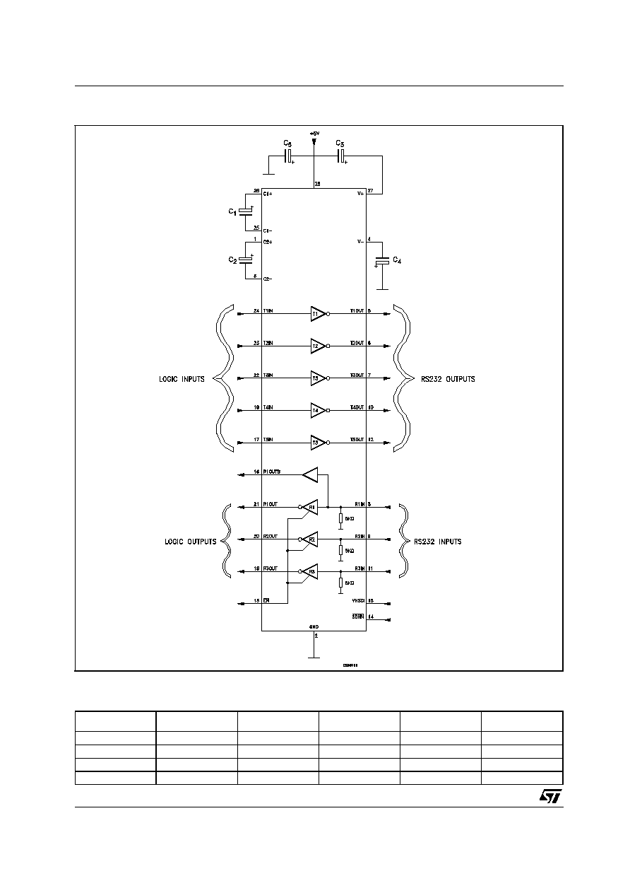
APPLICATION CIRCUITS
CAPACITANCE VALUE (
Ķ
F)
V
CC
C1
C2
C3
C4
Cbypass
3.0 to 3.6
0.22
0.22
0.22
0.22
0.1
3.1 to 3.6
0.1
0.1
0.1
0.1
0.1
4.5 to 5.5
0.047
0.33
0.33
0.33
0.1
3.0 to 5.5
0.22
0.1
0.1
0.1
0.1
ST3237E
7/13
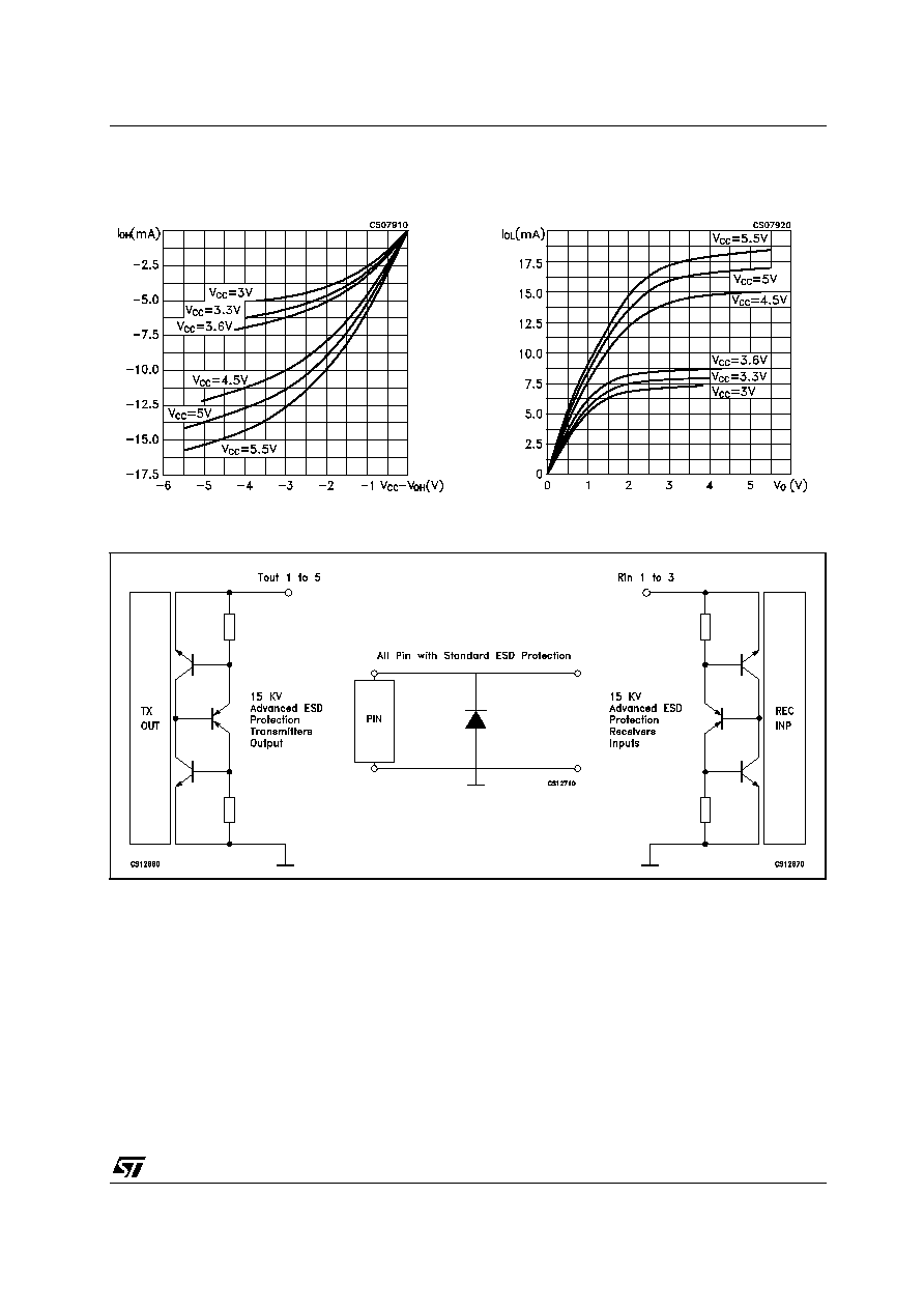
TYPICAL PERFORMANCE CHARACTERISTICS (unless otherwise specified T
j
= 25įC)
Figure 1 : LOW Level Receiver Output Current
Figure 2 : HIGH Level Receiver Output Current
ESD PROTECTION
Note: The High ESD protected pins are the I/O RS232 line, transmitter out and receiver in. The other pins guarantee Ī 2KV HBM ESD pro-
tection versus ground by means of diodes.
ST3237E
8/13
APPLICATION NOTE
This application note describes the procedure for determining the susceptibility and the test method to
verify ST ESD advanced protection on RS-232 or RS485 I/O device.
Static electricity is defined as an electrical charge caused by an imbalance of electrons on the surface of
a material. This imbalance of electrons produces an electric field that can be measured and that can
influence other objects at a distance. Electrostatic discharge is defined as the transfer of charge between
bodies at different electrical potentials. Electrostatic discharge (ESD) can change the electrical
characteristics of a semiconductor device, degrading or destroying it. Any input or output port (I/O) allows
access communication with other pieces of equipment by external connectors. These connectors are
directly linked by the I/O pins of RS-232 or RS485 interface. ST provides the E-series by advanced high
ESD protection structure. The protection functionality is tested in two different conditions:
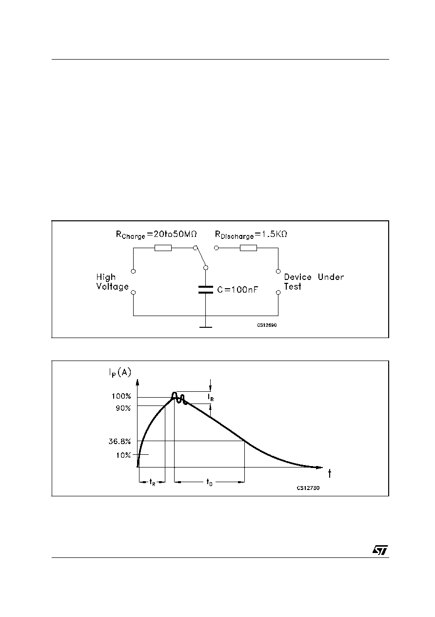
The first model is used to simulate the HUMAN BODY MODEL (HBM) event. A similar discharge can
occur from a charged conductive object, such as a metallic tool or fixture. The model used to characterize
this event is known as the Machine Model. A Human Body Model circuit and waveform is presented in
Figures below.
HUMAN BODY MODEL CIRCUIT
HUMAN BODY MODEL CURRENT WAVEFORM
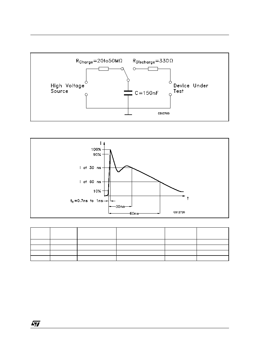
The second model is IEC 1000-4-2 and is used to simulate the reaction of the device on equipment when
subjected to electrostatic discharges, which may occur from personnel to objects near vital
instrumentation. Direct (Contact) and indirect (Air Gap) applications of discharges to the equipment under
test (EUT) are possible. Test characteristics are shown in circuit, waveform and table below.
ST3237E
9/13
IEC 1000-4-2 CIRCUIT
IEC 1000-4-2 CURRENT WAVEFORM
CHARACTERISTICS OF THE ESD GENERATOR
Level
Indicated
Voltage
First Peak Current of
Discharge (Ī 10%)
Rise Time With Discharge
Switch
Current at 30 ns
(Ī 30%)
Current at 60 ns
(Ī 30%)
1
2 KV
7.5 A
0.7 to 1ns
4 A
2 A
2
4 KV
15 A
0.7 to 1ns
8 A
4 A
3
6 KV
22.5 A
0.7 to 1ns
12 A
6 A
4
8 KV
30 A
0.7 to 1ns
16 A
8 A
ST3237E
10/13
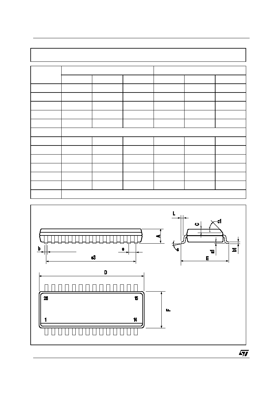
DIM.
mm.
inch
MIN.
TYP
MAX.
MIN.
TYP.
MAX.
A
2.65
0.104
a1
0.1
0.3
0.004
0.012
b
0.35
0.49
0.014
0.019
b1
0.23
0.32
0.009
0.012
C
0.5
0.020
c1
45į (typ.)
D
17.70
18.10
0.697
0.713
E
10.00
10.65
0.393
0.419
e
1.27
0.050
e3
16.51
0.650
F
7.40
7.60
0.291
0.300
L
0.50
1.27
0.020
0.050
S
į (max.)
SO-28 MECHANICAL DATA
0016023
8
ST3237E
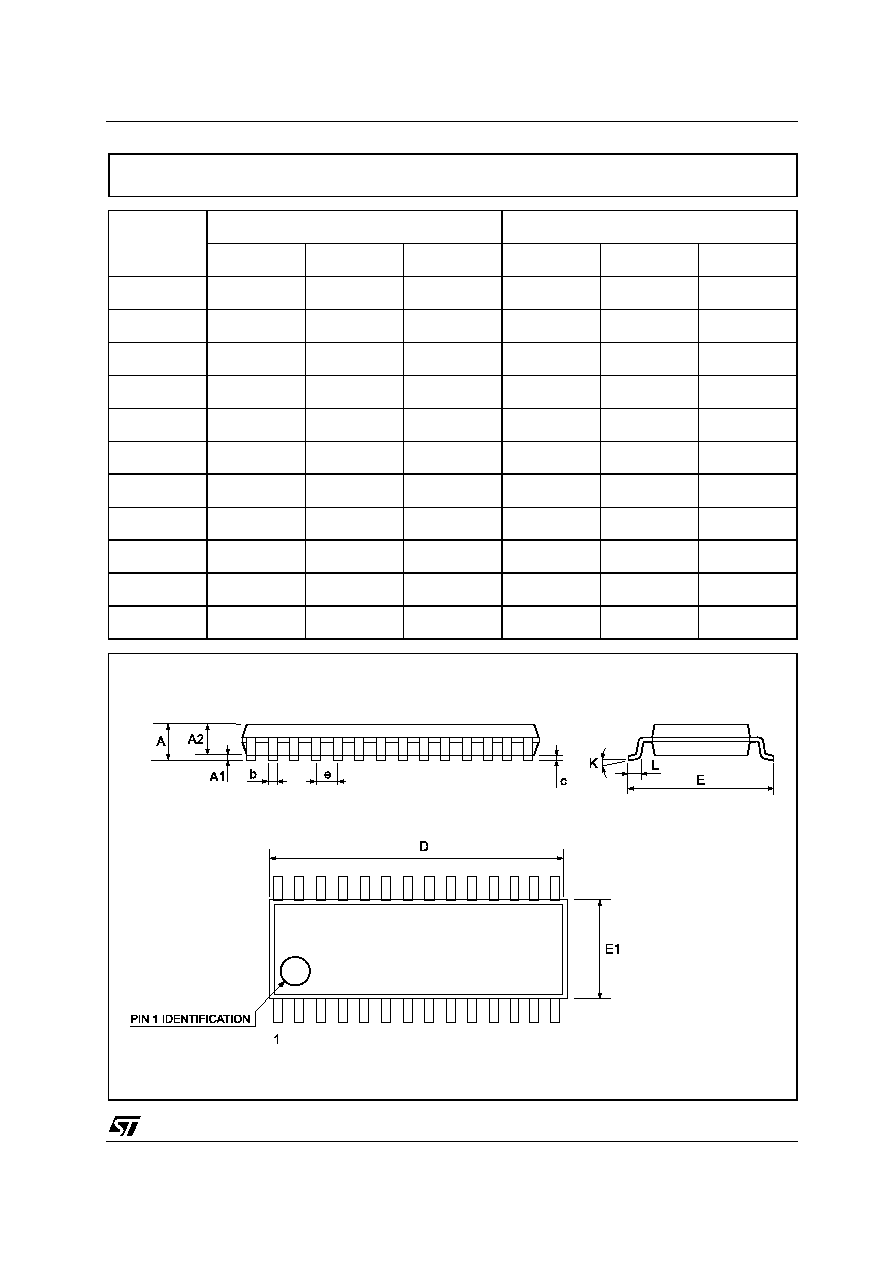
11/13
DIM.
mm.
inch
MIN.
TYP
MAX.
MIN.
TYP.
MAX.
A
2
0.079
A1
0.050
0.002
A2
1.65
1.75
1.85
0.065
0.069
0.073
b
0.22
0.38
0.009
0.015
c
0.09
0.25
0.004
0.010
D
9.9
10.2
10.5
0.390
0.402
0.413
E
7.4
7.8
8.2
0.291
0.307
0.323
E1
5
5.3
5.6
0.197
0.209
0.220
e
0.65 BSC
0.0256 BSC
K
0į
10į
0į
10į
L
0.55
0.75
0.95
0.022
0.030
0.037
SSOP28 MECHANICAL DATA
ST3237E
12/13
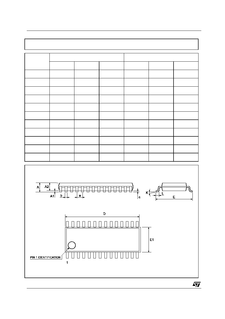
DIM.
mm.
inch
MIN.
TYP
MAX.
MIN.
TYP.
MAX.
A
1.2
0.047
A1
0.05
0.15
0.002
0.004
0.006
A2
0.8
1
1.05
0.031
0.039
0.041
b
0.19
0.30
0.007
0.012
c
0.09
0.20
0.004
0.0079
D
9.6
9.7
9.8
0.378
0.382
0.386
E
6.2
6.4
6.6
0.244
0.252
0.260
E1
4.3
4.4
4.48
0.169
0.173
0.176
e
0.65 BSC
0.0256 BSC
K
0į
8į
0į
8į
L
0.45
0.60
0.75
0.018
0.024
0.030
TSSOP28 MECHANICAL DATA
0128292B

ST3237E
13/13
Information furnished is believed to be accurate and reliable. However, STMicroelectronics assumes no responsibility for the
consequences of use of such information nor for any infringement of patents or other rights of third parties which may result from
its use. No license is granted by implication or otherwise under any patent or patent rights of STMicroelectronics. Specifications
mentioned in this publication are subject to change without notice. This publication supersedes and replaces all information
previously supplied. STMicroelectronics products are not authorized for use as critical components in life support devices or
systems without express written approval of STMicroelectronics.
© The ST logo is a registered trademark of STMicroelectronics
© 2003 STMicroelectronics - Printed in Italy - All Rights Reserved
STMicroelectronics GROUP OF COMPANIES
Australia - Brazil - Canada - China - Finland - France - Germany - Hong Kong - India - Israel - Italy - Japan - Malaysia - Malta - Morocco
Singapore - Spain - Sweden - Switzerland - United Kingdom - United States.
© http://www.st.com