 | –≠–ª–µ–∫—Ç—Ä–æ–Ω–Ω—ã–π –∫–æ–º–ø–æ–Ω–µ–Ω—Ç: 93C56 | –°–∫–∞—á–∞—Ç—å:  PDF PDF  ZIP ZIP |
Document Outline
- FEATURES SUMMARY
- MEMORY ORGANIZATION
- POWER-ON DATA PROTECTION
- INSTRUCTIONS
- READY/BUSY STATUS
- COMMON I/O OPERATION
- CLOCK PULSE COUNTER
- MAXIMUM RATING
- DC AND AC PARAMETERS
- PACKAGE MECHANICAL
- Figure 12. PDIP8 Ö 8 pin Plastic DIP, 0.25mm lead frame, Package Outline
- Table 24. PDIP8 Ö 8 pin Plastic DIP, 0.25mm lead frame, Package Mechanical Data
- Figure 13. SO8 narrow Ö 8 lead Plastic Small Outline, 150 mils body width, Package Outline
- Table 25. SO8 narrow Ö 8 lead Plastic Small Outline, 150 mils body width, Package Mechanical Data
- Figure 14. UFDFPN8 (MLP8) 8-lead Ultra thin Fine pitch Dual Flat Package No lead 2x3mm∑, Outline
- Table 26. UFDFPN8 (MLP8) 8-lead Ultra thin Fine pitch Dual Flat Package No lead 2x3mm∑, Data
- Figure 15. TSSOP8 3x3mm∑ Ö 8 lead Thin Shrink Small Outline, 3x3mm∑ body size, Package Outline
- Table 27. TSSOP8 3x3mm∑ Ö 8 lead Thin Shrink Small Outline, 3x3mm∑ body size, Mechanical Data
- Figure 16. TSSOP8 Ö 8 lead Thin Shrink Small Outline, Package Outline
- Table 28. TSSOP8 Ö 8 lead Thin Shrink Small Outline, Package Mechanical Data
- PART NUMBERING
- REVISION HISTORY
1/31
August 2004
M93C86, M93C76, M93C66
M93C56, M93C46
16Kbit, 8Kbit, 4Kbit, 2Kbit and 1Kbit (8-bit or 16-bit wide)
MICROWIREÆ Serial Access EEPROM
FEATURES SUMMARY
s
Industry Standard MICROWIRE Bus
s
Single Supply Voltage:
≠
4.5 to 5.5V for M93Cx6
≠
2.5 to 5.5V for M93Cx6-W
≠
1.8 to 5.5V for M93Cx6-R
s
Dual Organization: by Word (x16) or Byte (x8)
s
Programming Instructions that work on: Byte,
Word or Entire Memory
s
Self-timed Programming Cycle with Auto-
Erase
s
Ready/Busy Signal During Programming
s
Speed:
≠
1MHz Clock Rate, 10ms Write Time
(Current product, identified by process
identification letter F or M)
≠
2MHz Clock Rate, 5ms Write Time (New
Product, identified by process
identification letter W or G or S)
s
Sequential Read Operation
s
Enhanced ESD/Latch-Up Behaviour
s
More than 1 Million Erase/Write Cycles
s
More than 40 Year Data Retention
Table 1. Product List
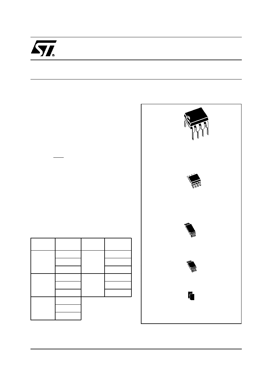
Figure 1. Packages
Reference
Part
Number
Reference
Part
Number
M93C86
M93C86
M93C56
M93C56
M93C86-W
M93C56-W
M93C86-R
M93C56-R
M93C76
M93C76
M93C46
M93C46
M93C76-W
M93C46-W
M93C76-R
M93C46-R
M93C66
M93C66
M93C66-W
M93C66-R
PDIP8 (BN)
SO8 (MN)
150 mil width
8
1
TSSOP8 (DW)
169 mil width
TSSOP8 (DS)
3x3mm≤ body size (MSOP)
8
1
UFDFPN8 (MB)
2x3mm≤ (MLP)

M93C86, M93C76, M93C66, M93C56, M93C46
2/31
TABLE OF CONTENTS
FEATURES SUMMARY . . . . . . . . . . . . . . . . . . . . . . . . . . . . . . . . . . . . . . . . . . . . . . . . . . . . . . . . . . . . . 1
Table 1. Product List . . . . . . . . . . . . . . . . . . . . . . . . . . . . . . . . . . . . . . . . . . . . . . . . . . . . . . . . . . . . 1
Figure 1. Packages . . . . . . . . . . . . . . . . . . . . . . . . . . . . . . . . . . . . . . . . . . . . . . . . . . . . . . . . . . . . . . 1
Figure 2. Logic Diagram . . . . . . . . . . . . . . . . . . . . . . . . . . . . . . . . . . . . . . . . . . . . . . . . . . . . . . . . . . 4
Table 2. Signal Names . . . . . . . . . . . . . . . . . . . . . . . . . . . . . . . . . . . . . . . . . . . . . . . . . . . . . . . . . . 4
Table 3. Memory Size versus Organization. . . . . . . . . . . . . . . . . . . . . . . . . . . . . . . . . . . . . . . . . . . 4
Table 4. Instruction Set for the M93Cx6 . . . . . . . . . . . . . . . . . . . . . . . . . . . . . . . . . . . . . . . . . . . . . 4
Figure 3. DIP, SO, TSSOP and MLP Connections (Top View). . . . . . . . . . . . . . . . . . . . . . . . . . . . . 5
MEMORY ORGANIZATION . . . . . . . . . . . . . . . . . . . . . . . . . . . . . . . . . . . . . . . . . . . . . . . . . . . . . . . . . . 5
POWER-ON DATA PROTECTION . . . . . . . . . . . . . . . . . . . . . . . . . . . . . . . . . . . . . . . . . . . . . . . . . . . . . 5
INSTRUCTIONS . . . . . . . . . . . . . . . . . . . . . . . . . . . . . . . . . . . . . . . . . . . . . . . . . . . . . . . . . . . . . . . . . . . 6
Table 5. Instruction Set for the M93C46 . . . . . . . . . . . . . . . . . . . . . . . . . . . . . . . . . . . . . . . . . . . . . 6
Table 6. Instruction Set for the M93C56 and M93C66 . . . . . . . . . . . . . . . . . . . . . . . . . . . . . . . . . . 7
Table 7. Instruction Set for the M93C76 and M93C86 . . . . . . . . . . . . . . . . . . . . . . . . . . . . . . . . . . 7
Read . . . . . . . . . . . . . . . . . . . . . . . . . . . . . . . . . . . . . . . . . . . . . . . . . . . . . . . . . . . . . . . . . . . . . . . . . 8
Erase/Write Enable and Disable . . . . . . . . . . . . . . . . . . . . . . . . . . . . . . . . . . . . . . . . . . . . . . . . . . . 8
Figure 4. READ, WRITE, EWEN, EWDS Sequences. . . . . . . . . . . . . . . . . . . . . . . . . . . . . . . . . . . . 8
Erase . . . . . . . . . . . . . . . . . . . . . . . . . . . . . . . . . . . . . . . . . . . . . . . . . . . . . . . . . . . . . . . . . . . . . . . . . 9
Write . . . . . . . . . . . . . . . . . . . . . . . . . . . . . . . . . . . . . . . . . . . . . . . . . . . . . . . . . . . . . . . . . . . . . . . . . 9
Figure 5. ERASE, ERAL Sequences . . . . . . . . . . . . . . . . . . . . . . . . . . . . . . . . . . . . . . . . . . . . . . . . 9
Erase All . . . . . . . . . . . . . . . . . . . . . . . . . . . . . . . . . . . . . . . . . . . . . . . . . . . . . . . . . . . . . . . . . . . . . 10
Write All . . . . . . . . . . . . . . . . . . . . . . . . . . . . . . . . . . . . . . . . . . . . . . . . . . . . . . . . . . . . . . . . . . . . . 10
Figure 6. WRAL Sequence . . . . . . . . . . . . . . . . . . . . . . . . . . . . . . . . . . . . . . . . . . . . . . . . . . . . . . . 10
READY/BUSY STATUS . . . . . . . . . . . . . . . . . . . . . . . . . . . . . . . . . . . . . . . . . . . . . . . . . . . . . . . . . . . . 11
COMMON I/O OPERATION . . . . . . . . . . . . . . . . . . . . . . . . . . . . . . . . . . . . . . . . . . . . . . . . . . . . . . . . . 11
CLOCK PULSE COUNTER . . . . . . . . . . . . . . . . . . . . . . . . . . . . . . . . . . . . . . . . . . . . . . . . . . . . . . . . . 11
Figure 7. Write Sequence with One Clock Glitch . . . . . . . . . . . . . . . . . . . . . . . . . . . . . . . . . . . . . . 11
MAXIMUM RATING. . . . . . . . . . . . . . . . . . . . . . . . . . . . . . . . . . . . . . . . . . . . . . . . . . . . . . . . . . . . . . . . 12
Table 8. Absolute Maximum Ratings . . . . . . . . . . . . . . . . . . . . . . . . . . . . . . . . . . . . . . . . . . . . . . . 12
DC AND AC PARAMETERS. . . . . . . . . . . . . . . . . . . . . . . . . . . . . . . . . . . . . . . . . . . . . . . . . . . . . . . . . 13
Table 9. Operating Conditions (M93Cx6) . . . . . . . . . . . . . . . . . . . . . . . . . . . . . . . . . . . . . . . . . . . 13
Table 10. Operating Conditions (M93Cx6-W) . . . . . . . . . . . . . . . . . . . . . . . . . . . . . . . . . . . . . . . . . 13
Table 11. Operating Conditions (M93Cx6-R) . . . . . . . . . . . . . . . . . . . . . . . . . . . . . . . . . . . . . . . . . 13
Table 12. AC Measurement Conditions (M93Cx6) . . . . . . . . . . . . . . . . . . . . . . . . . . . . . . . . . . . . . 14
Table 13. AC Measurement Conditions (M93Cx6-W and M93Cx6-R) . . . . . . . . . . . . . . . . . . . . . . 14
Figure 8. AC Testing Input Output Waveforms . . . . . . . . . . . . . . . . . . . . . . . . . . . . . . . . . . . . . . . . 14

3/31
M93C86, M93C76, M93C66, M93C56, M93C46
Table 14. Capacitance. . . . . . . . . . . . . . . . . . . . . . . . . . . . . . . . . . . . . . . . . . . . . . . . . . . . . . . . . . . 14
Table 15. DC Characteristics (M93Cx6, Device Grade 6) . . . . . . . . . . . . . . . . . . . . . . . . . . . . . . . . 15
Table 16. DC Characteristics (M93Cx6, Device Grade 7 or 3) . . . . . . . . . . . . . . . . . . . . . . . . . . . . 15
Table 17. DC Characteristics (M93Cx6-W, Device Grade 6) . . . . . . . . . . . . . . . . . . . . . . . . . . . . . 16
Table 18. DC Characteristics (M93Cx6-W, Device Grade 7 or 3) . . . . . . . . . . . . . . . . . . . . . . . . . . 17
Table 19. DC Characteristics (M93Cx6-R) . . . . . . . . . . . . . . . . . . . . . . . . . . . . . . . . . . . . . . . . . . . 17
Table 20. AC Characteristics (M93Cx6, Device Grade 6, 7 or 3) . . . . . . . . . . . . . . . . . . . . . . . . . . 18
Table 21. AC Characteristics (M93Cx6-W, Device Grade 6). . . . . . . . . . . . . . . . . . . . . . . . . . . . . . 19
Table 22. AC Characteristics (M93Cx6-W, Device Grade 7 or 3) . . . . . . . . . . . . . . . . . . . . . . . . . . 20
Table 23. AC Characteristics (M93Cx6-R) . . . . . . . . . . . . . . . . . . . . . . . . . . . . . . . . . . . . . . . . . . . 21
Figure 9. Synchronous Timing (Start and Op-Code Input) . . . . . . . . . . . . . . . . . . . . . . . . . . . . . . . 22
Figure 10.Synchronous Timing (Read or Write) . . . . . . . . . . . . . . . . . . . . . . . . . . . . . . . . . . . . . . . 22
Figure 11.Synchronous Timing (Read or Write) . . . . . . . . . . . . . . . . . . . . . . . . . . . . . . . . . . . . . . . 22
PACKAGE MECHANICAL . . . . . . . . . . . . . . . . . . . . . . . . . . . . . . . . . . . . . . . . . . . . . . . . . . . . . . . . . . 23
Figure 12.PDIP8 ≠ 8 pin Plastic DIP, 0.25mm lead frame, Package Outline . . . . . . . . . . . . . . . . . 23
Table 24. PDIP8 ≠ 8 pin Plastic DIP, 0.25mm lead frame, Package Mechanical Data . . . . . . . . . . 23
Figure 13.SO8 narrow ≠ 8 lead Plastic Small Outline, 150 mils body width, Package Outline . . . . 24
Table 25. SO8 narrow ≠ 8 lead Plastic Small Outline, 150 mils body width, Package Mechanical Data
24
Figure 14.UFDFPN8 (MLP8) 8-lead Ultra thin Fine pitch Dual Flat Package No lead 2x3mm≤, Outline
25
Table 26. UFDFPN8 (MLP8) 8-lead Ultra thin Fine pitch Dual Flat Package No lead 2x3mm≤, Data .
25
Figure 15.TSSOP8 3x3mm≤ ≠ 8 lead Thin Shrink Small Outline, 3x3mm≤ body size, Package Outline
26
Table 27. TSSOP8 3x3mm≤ ≠ 8 lead Thin Shrink Small Outline, 3x3mm≤ body size, Mechanical Data
26
Figure 16.TSSOP8 ≠ 8 lead Thin Shrink Small Outline, Package Outline . . . . . . . . . . . . . . . . . . . 27
Table 28. TSSOP8 ≠ 8 lead Thin Shrink Small Outline, Package Mechanical Data . . . . . . . . . . . . 27
PART NUMBERING . . . . . . . . . . . . . . . . . . . . . . . . . . . . . . . . . . . . . . . . . . . . . . . . . . . . . . . . . . . . . . . 28
Table 29. Ordering Information Scheme . . . . . . . . . . . . . . . . . . . . . . . . . . . . . . . . . . . . . . . . . . . . . 28
Table 30. How to Identify Current and New Products by the Process Identification Letter . . . . . . . 29
REVISION HISTORY . . . . . . . . . . . . . . . . . . . . . . . . . . . . . . . . . . . . . . . . . . . . . . . . . . . . . . . . . . . . . . . 30
Table 31. Document Revision History . . . . . . . . . . . . . . . . . . . . . . . . . . . . . . . . . . . . . . . . . . . . . . . 30
M93C86, M93C76, M93C66, M93C56, M93C46
4/31
SUMMARY DESCRIPTION
These electrically erasable programmable memo-
ry (EEPROM) devices are accessed through a Se-
rial Data Input (D) and Serial Data Output (Q)
using the MICROWIRE bus protocol.
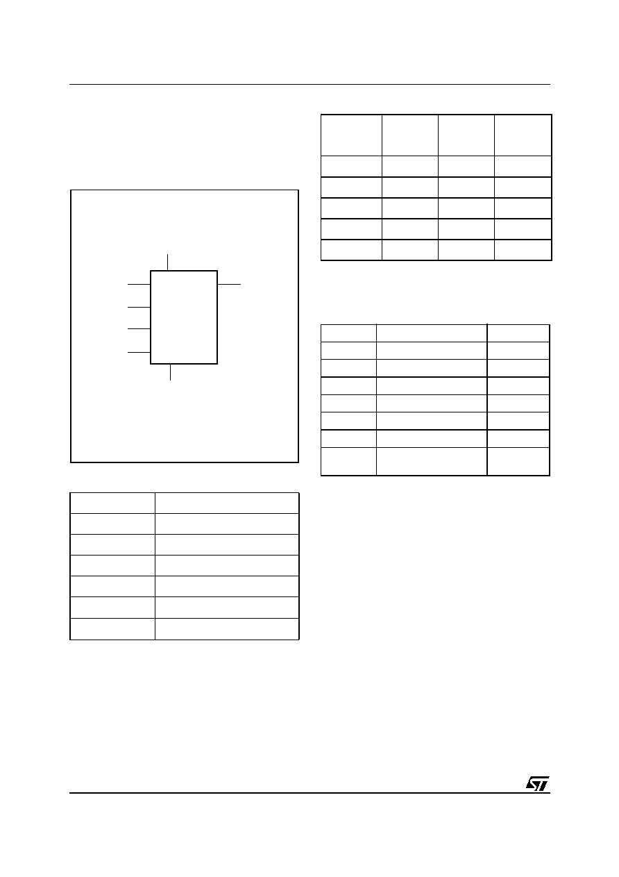
Figure 2. Logic Diagram
Table 2. Signal Names
The memory array organization may be divided
into either bytes (x8) or words (x16) which may be
selected by a signal applied on Organization Se-
lect (ORG). The bit, byte and word sizes of the
memories are as shown in
Table 3.
.
Table 3. Memory Size versus Organization
The M93Cx6 is accessed by a set of instructions,
as summarized in
Table 4.
, and in more detail in
Table 5.
to
Table 7.
).
Table 4. Instruction Set for the M93Cx6
A Read Data from Memory (READ) instruction
loads the address of the first byte or word to be
read in an internal address register. The data at
this address is then clocked out serially. The ad-
dress register is automatically incremented after
the data is output and, if Chip Select Input (S) is
held High, the M93Cx6 can output a sequential
stream of data bytes or words. In this way, the
memory can be read as a data stream from eight
to 16384 bits long (in the case of the M93C86), or
continuously (the address counter automatically
rolls over to 00h when the highest address is
reached).
Programming is internally self-timed (the external
clock signal on Serial Clock (C) may be stopped or
left running after the start of a Write cycle) and
does not require an Erase cycle prior to the Write
instruction. The Write instruction writes 8 or 16 bits
at a time into one of the byte or word locations of
the M93Cx6. After the start of the programming cy-
cle, a Busy/Ready signal is available on Serial
Data Output (Q) when Chip Select Input (S) is driv-
en High.
S
Chip Select Input
D
Serial Data Input
Q
Serial Data Output
C
Serial Clock
ORG
Organisation Select
V
CC
Supply Voltage
V
SS
Ground
AI01928
D
VCC
M93Cx6
VSS
C
Q
S
ORG
Device
Number
of Bits
Number
of 8-bit
Bytes
Number
of 16-bit
Words
M93C86
16384
2048
1024
M93C76
8192
1024
512
M93C66
4096
512
256
M93C56
2048
256
128
M93C46
1024
128
64
Instruction
Description
Data
READ
Read Data from Memory
Byte or Word
WRITE
Write Data to Memory
Byte or Word
EWEN
Erase/Write Enable
EWDS
Erase/Write Disable
ERASE
Erase Byte or Word
Byte or Word
ERAL
Erase All Memory
WRAL
Write All Memory
with same Data
5/31
M93C86, M93C76, M93C66, M93C56, M93C46
An internal Power-on Data Protection mechanism
in the M93Cx6 inhibits the device when the supply
is too low.
Figure 3. DIP, SO, TSSOP and MLP
Connections (Top View)
Note: 1. See
PACKAGE MECHANICAL
section for package di-
mensions, and how to identify pin-1.
2. DU = Don't Use.
The DU (Don't Use) pin does not contribute to the
normal operation of the device. It is reserved for
use by STMicroelectronics during test sequences.
The pin may be left unconnected or may be con-
nected to V
CC
or V
SS
. Direct connection of DU to
V
SS
is recommended for the lowest stand-by pow-
er consumption.
MEMORY ORGANIZATION
The M93Cx6 memory is organized either as bytes
(x8) or as words (x16). If Organization Select
(ORG) is left unconnected (or connected to V
CC
)
the x16 organization is selected; when Organiza-
tion Select (ORG) is connected to Ground (V
SS
)
the x8 organization is selected. When the M93Cx6
is in stand-by mode, Organization Select (ORG)
should be set either to V
SS
or V
CC
for minimum
power consumption. Any voltage between V
SS
and V
CC
applied to Organization Select (ORG)
may increase the stand-by current.
POWER-ON DATA PROTECTION
To prevent data corruption and inadvertent write
operations during power-up, a Power-On Reset
(POR) circuit resets all internal programming cir-
cuitry, and sets the device in the Write Disable
mode.
≠
At Power-up and Power-down, the device
must not be selected (that is, Chip Select Input
(S) must be driven Low) until the supply
voltage reaches the operating value V
CC
specified in
Table 9.
to
Table 11.
.
≠
When V
CC
reaches its valid level, the device is
properly reset (in the Write Disable mode) and
is ready to decode and execute incoming
instructions.
For the M93Cx6 devices (5V range) the POR
threshold voltage is around 3V. For the M93Cx6-
W (3V range) and M93Cx6-R (2V range) the POR
threshold voltage is around 1.5V.
VSS
Q
ORG
DU
C
S
VCC
D
AI01929B
M93Cx6
1
2
3
4
8
7
6
5