 | ÐлекÑÑоннÑй компоненÑ: A888AT | СкаÑаÑÑ:  PDF PDF  ZIP ZIP |
MULTI-BAND RF FREQUENCY SYNTHESIZER WITH
1/21
A888AT
GreenRFS
February 2005
This is preliminary information on a new product now in development. Details are subject to change without notice.
1
FEATURES
Integer-N Frequency Synthesizer
Dual differential integrated VCOs with
automatic center frequency calibration:
Direct Output:
3280 3900 MHz
3800 4400 MHz
Internal divider by 2:
1640 1950 MHz
1900 2200 MHz
Internal divider by 4:
820 975 MHz
950 1100 MHz
Fast lock time: 150
µs
Dual modulus prescaler (64/65) and 2
programmable counters to achieve a feedback
division ratio from 4096 to 32767.
Programmable reference frequency divider (9
bits)
Phase frequency comparator and charge pump
Programmable charge pump current
Digital Lock Detector
I
2
C bus interface with 3 bit programmable
address (1100A
2
A
1
A
0
)
Power down mode
Small size exposed pad VFQFPN28 package
5x5x1.0mm
Process: BICMOS 0.35
µm SiGe
2
DESCRIPTION
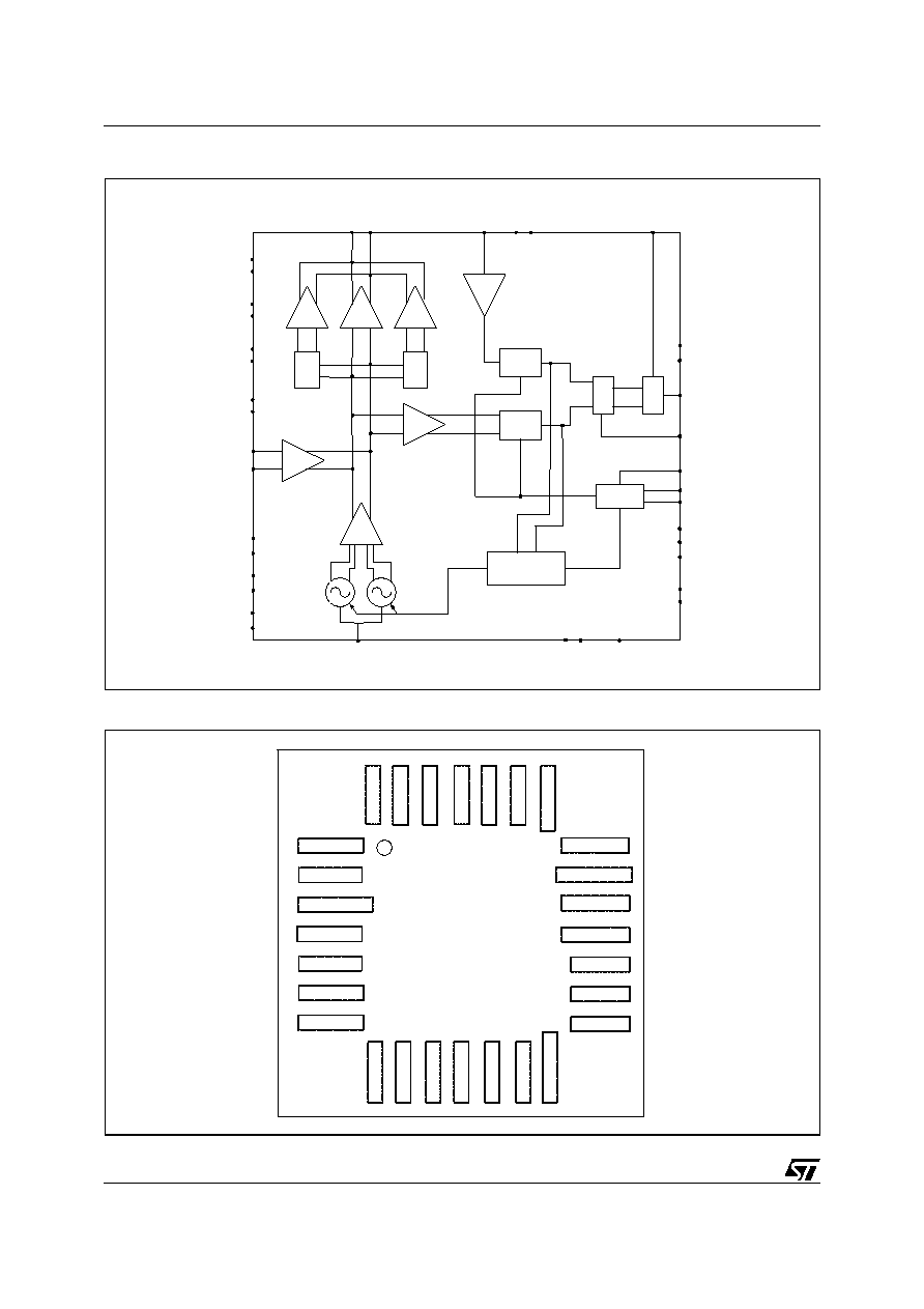
The STMicroelectronics GreenRFS is an integrat-
ed RF synthesizer and voltage controlled oscilla-
tors (VCOs).
Showing high performance, high integration, low
power, and multi-band performances, GreenRFS
is a low cost one chip alternative to discrete PLL
and VCOs solutions.
GreenRFS includes an Integer-N frequency syn-
thesizer and two VCOs.
Each VCO provides a low phase noise floor of
-151dBc/Hz and an automatic center frequency
calibration in order to cover the 3280MHz-
4400MHz (direct output), the 1640MHz-2200MHz
(with internal divider by 2) and the 820MHz-
1100MHz (with internal divider by 4) bands.
The GreenRFS is designed with STMicroelectron-
ics advanced 0.35
µm SiGe process.
3
APPLICATIONS
Cellular 3G Infrastructure Equipment
Other Wireless Communication Systems
PRELIMINARY DATA
MULTI-BAND RF FREQUENCY SYNTHESIZER WITH
INTEGRATED VCO
S
Rev. 1
Figure 1. Package
Table 1. Order Codes
Part Number
Package
A888AT
VFQFPN28
A888ATR
Tape & Reel
VFQFPN28
GreenRFS - A888AT
2/21
Figure 2. Block Diagram
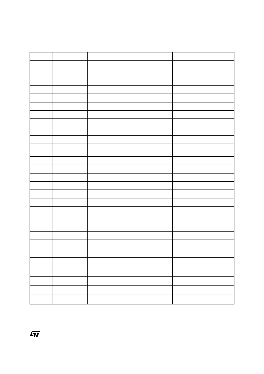
Figure 3. Pin Connections
VCO
BUFF
VDD_VCO1
VC
T
R
L
EXTVCO_INN
EXTVCO_INP
DI
V
4
DI
V
2
OU
T
B
U
F
P
D
IV
4
B
UF
D
IV
2
B
UF
EXT
VCO BUF
VSS_VCO1
VDD_VCO2
VSS_VCO2
VDD_BUFVCO
VSS_BUFVCO
VDD_OUTBUF
VSS_OUTBUF
VDD_DIV4
VSS_DIV4
VDD_DIV2
VSS_DIV2
OU
T
B
UF
N
VDD_ESD
VSS_ESD
ADD0
ADD1
ADD2
VDD_I2C
VSS_I2C
VCO
Divider
REF
Divider
BUF
P
F
D
C
P
UP
DN
ICP
LOCK_DET
VS
S
_
P
L
L
VD
D
_
P
L
L
RE
XT
RE
F
_
I
N
BUF
VDD_CP
VSS_CP
I²C BUS
SDA
SCL
TE
S
T
2
TE
S
T
1
EX
T
_
P
D
ATPGON
VCO
Calibrator
VC
O
B
U
F
VCO
BUFF
VDD_VCO1
VC
T
R
L
EXTVCO_INN
EXTVCO_INP
DI
V
4
DI
V
2
OU
T
B
U
F
P
D
IV
4
B
UF
D
IV
2
B
UF
EXT
VCO BUF
VSS_VCO1
VDD_VCO2
VSS_VCO2
VDD_BUFVCO
VSS_BUFVCO
VDD_OUTBUF
VSS_OUTBUF
VDD_DIV4
VSS_DIV4
VDD_DIV2
VSS_DIV2
OU
T
B
UF
N
VDD_ESD
VSS_ESD
ADD0
ADD1
ADD2
VDD_I2C
VSS_I2C
VCO
Divider
REF
Divider
BUF
P
F
D
C
P
UP
DN
ICP
LOCK_DET
VS
S
_
VCO
BUFF
VDD_VCO1
VC
T
R
L
EXTVCO_INN
EXTVCO_INP
DI
V
4
DI
V
2
OU
T
B
U
F
P
D
IV
4
B
UF
D
IV
2
B
UF
EXT
VCO BUF
VSS_VCO1
VDD_VCO2
VSS_VCO2
VDD_BUFVCO
VSS_BUFVCO
VDD_OUTBUF
VSS_OUTBUF
VDD_DIV4
VSS_DIV4
VDD_DIV2
VSS_DIV2
OU
T
B
UF
N
VDD_ESD
VSS_ESD
ADD0
ADD1
ADD2
VDD_I2C
VSS_I2C
VCO
Divider
REF
Divider
BUF
P
F
D
C
P
UP
DN
ICP
LOCK_DET
VS
S
_
P
L
L
VD
D
_
P
L
L
RE
XT
RE
F
_
I
N
BUF
VDD_CP
VSS_CP
I²C BUS
SDA
SCL
TE
S
T
2
TE
S
T
1
EX
T
_
P
D
ATPGON
VCO
Calibrator
VC
O
B
U
F
QFN 28
OUTBUFN
VDD_DIV4
VDD_DIV2
VDD_OUTBUF
SC
L
AD
D
1
VD
D
_I
2
C
VDD_BUFVCO
EXTVCO_INN
VDD_PLL
I
CP
RE
X
T
TEST2
V
DD_
ES
D
VC
T
R
L
VDD_VCO2
REF_IN
VDD_VCO1
VD
D_
CP
TE
S
T
1
L
O
CK
_D
E
T
ATPGON
AD
D
0
AD
D
2
EX
T
_
PD
OUTBUFP
S
DA
EXTVCO_INP
QFN 28
OUTBUFN
VDD_DIV4
VDD_DIV2
VDD_OUTBUF
SC
L
AD
D
1
VD
D
_I
2
C
VDD_BUFVCO
EXTVCO_INN
VDD_PLL
I
CP
RE
X
T
TEST2
V
DD_
ES
D
VC
T
R
L
VDD_VCO2
REF_IN
VDD_VCO1
VD
D_
CP
TE
S
T
1
L
O
CK
_D
E
T
ATPGON
AD
D
0
AD
D
2
EX
T
_
PD
OUTBUFP
S
DA
EXTVCO_INP
3/21
GreenRFS - A888AT
Table 2. Pin Description
Pin No
Name
Description
Observations
1
VDD_VCO1
VCO power supply
2
VDD_DIV2
Divider by 2 power supply
3
VDD_OUTBUF
Output buffer power supply
4
OUTBUFP
LO buffer positive output
Open collector
5
OUTBUFN
LO buffer negative output
Open collector
6
VDD_DIV4
Divider by 4 power supply
7
VDD_VCO2
VCO power supply
8
VDD_ESD
ESD positive rail power supply
9
VCTRL
VCO control voltage
10
ICP
PLL charge pump output
11
REXT
External resistance connection for PLL charge
pump
12
VDD_CP
Power supply for charge pump
13
TEST1
Test input 1
Used only for testing purpose
14
LOCK_DET
Lock detector
CMOS Output
15
TEST2
Test input 2
Used only for testing purpose
16
REF_IN
Reference frequency input
17
VDD_PLL
PLL digital power supply
18
EXTVCO_INN
External VCO negative input
19
EXTVCO_INP
External VCO positive input
20
VDD_BUFVCO
VCO buffer power supply
21
ATPGON
SCAN mode activated
22
VDD_I
2
C
I
2
C bus power supply
23
EXT_PD
Power down hardware
CMOS Input
24
SDA
I
2
CBUS data line
CMOS Bidir Schmitt triggered
25
SCL
I
2
CBUS clock line
CMOS Input
26
ADD0
I
2
CBUS address select pin
CMOS Input
27
ADD1
I
2
CBUS address select pin
CMOS Input
28
ADD2
I
2
CBUS address select pin
CMOS Input
GreenRFS - A888AT
4/21
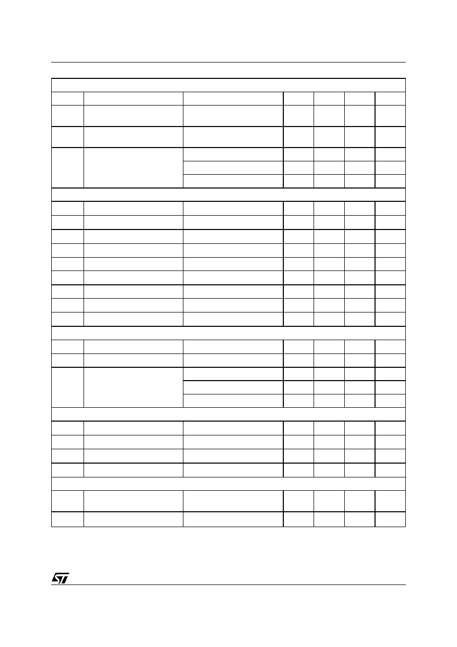
Table 3. Absolute Maximum Ratings
Table 4. Operating Conditions
Table 5. Digital Logic Level
4
ELECTRICAL CHARACTERISTCS
All Electrical Specifications are intended at 3.3V supply voltage and 25°C T
amb
unless otherwise specified
Table 6.
Symbol
Parameter
Values
Unit
AV
CC
Analog Supply voltage
0 to 4.6
V
DV
CC
Digital Supply voltage
0 to 4.6
V
T
stg
Storage temperature
+150
°C
ESD
Electrical Static Discharge
- HBM
- CDM-JEDEC Standard
2
0.5
KV
Symbol
Parameter
Test conditions
Min
Typ
Max
Unit
AV
CC
Analog Supply voltage
3.0
3.3
3.6
V
DV
CC
Digital Supply voltage
3.0
3.3
3.6
V
I
CC
Current Consumption
100
mA
T
amb
Operating ambient temperature
-40
85
°C
T
j
Maximum junction temperature
125
°C
R
th j-a
Junction to ambient package thermal
resistance
Multilayer JEDEC board
35
°C/W
Symbol
Parameter
Test conditions
Min
Typ
Max
Unit
V
il
Low level input voltage
0.2*Vdd
V
V
ih
High level input voltage
0.8*Vdd
V
V
hyst
Schmitt trigger hysteresis
0.8
V
V
ol
Low level output voltage
0.4
V
V
oh
High level output voltage
0.85*Vdd
V
Symbol
Parameter
Test Condition
Min
Typ
Max
Units
REFERENCE
f
ref
Reference input frequency
10
13
100
MHz
Reference input sensitivity
350
mVpp
f
comp
Comparison frequency
200
KHz
f
step
Frequency step
LO direct output
200
KHz
LO with Divider by 2
100
KHz
LO with Divider by 4
50
KHz
5/21
GreenRFS - A888AT
Notes: 1. : see relationship between ICP and REXT
2. : Comparison frequency leakage (400KHz) and harmonics
3. : 40 KHz PLL bandwidth
CHARGE PUMP
Symbol
Parameter
Test Condition
Min
Typ
Max
Units
I
CP
ICP sink/source
1
REXT= 9.1 k
; 3bit
programmable
250
1000
2000
µA
V
OCP
Output voltage compliance
range
0.4
V
dd
-0.3
V
Spurious
2
Direct Output
-65
-54
dBc
Divider by 2
-70
-60
dBc
Divider by 4
-70
-66
dBc
VCOs
I
VCO
Oscillator current consumption
25
mA
I
VCOBUF
VCO buffer consumption
15
mA
Kvco
A
VCOA sensitivity
70
MHz/V
Kvco
B
VCOB sensitivity
50
MHz/V
LO Harmonic Spurious
-20
dBc
V
TUN
VCO control voltage
0.4
3
V
Pushing
10
MHz/V
I
DIV4
DIVIDER by 4 consumption
14
mA
I
DIV2
DIVIDER by 2 consumption
18
mA
LO OUTPUT BUFFER
P
OUT
Output level
0
dBm
RL
Return Loss
Matched to 50ohm
15
dB
I
LOBUF
Current Consumption
DIV4 Buff
26
mA
DIV2 Buff
23
mA
Direct Output
37
mA
EXTERNAL VCO (Test purpose only)
f
INVCO
Frequency range
3.28
4.4
GHz
P
IN
Input level
0
+6
dBm
V
INDC
DC Input level
2
V
I
EXTBUF
Current Consumption
VCO Internal Buffer
15
mA
PLL MISCELLANEUS
I
PLL
Current Consumption
Input Buffer, Prescaler, Digital
Dividers, misc
10
mA
t
LOCK
Lock up time (lock to lock)
3
150
µs
Table 6. (continued)