1/8
ACS102-5Tx
PRELIMINARY DATASHEET
Æ
December 1999 - Ed: 4B
AC LINE SWITCH
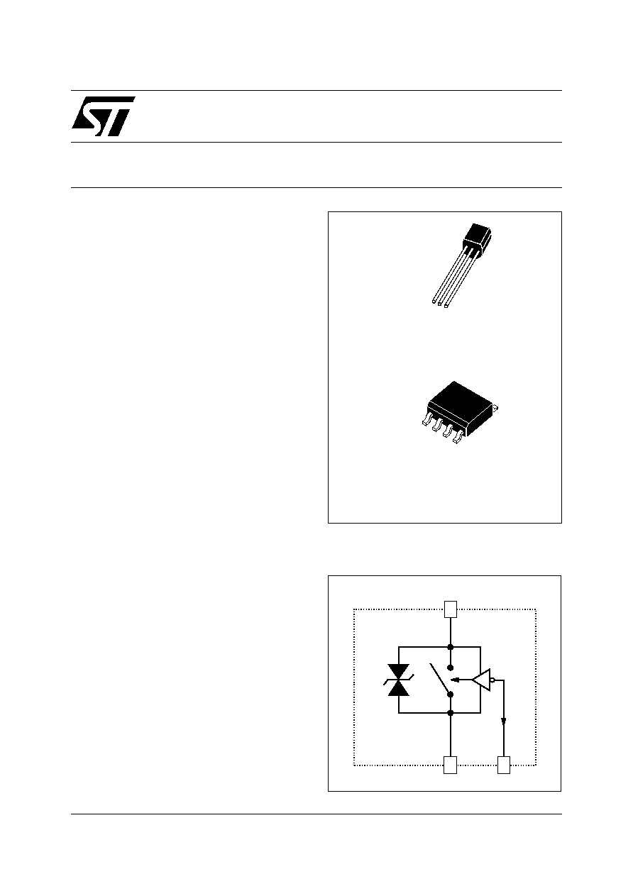
TO92
ACS102-5TA
n
Blocking voltage : V
DRM
/ V
RRM
= 500V
n
Clamping voltage : V
CL
= 600 V
n
Nominal current : I
T(RMS)
= 0.2 A
n
Gate triggering current : I
GT
< 5 mA
n
Switch integrated driver
n
SO-8 package:
- drive reference COM connected to 2 cooling pins
- 3 mm creepage distance from pin OUT to other pins
FEATURES
The ACS102 belongs to the AC line switch family
built around the ASD concept. This high perfor-
mance 5 mA switch circuit is able to control an up
to 0.3 A load.
The ACS switch embeds a high voltage clamping
structure to absorb the inductive turn off energy
and a gate level shifter driver to separate the digital
controller from the main switch. It is triggered with
a negative gate current flowing out of the gate pin.
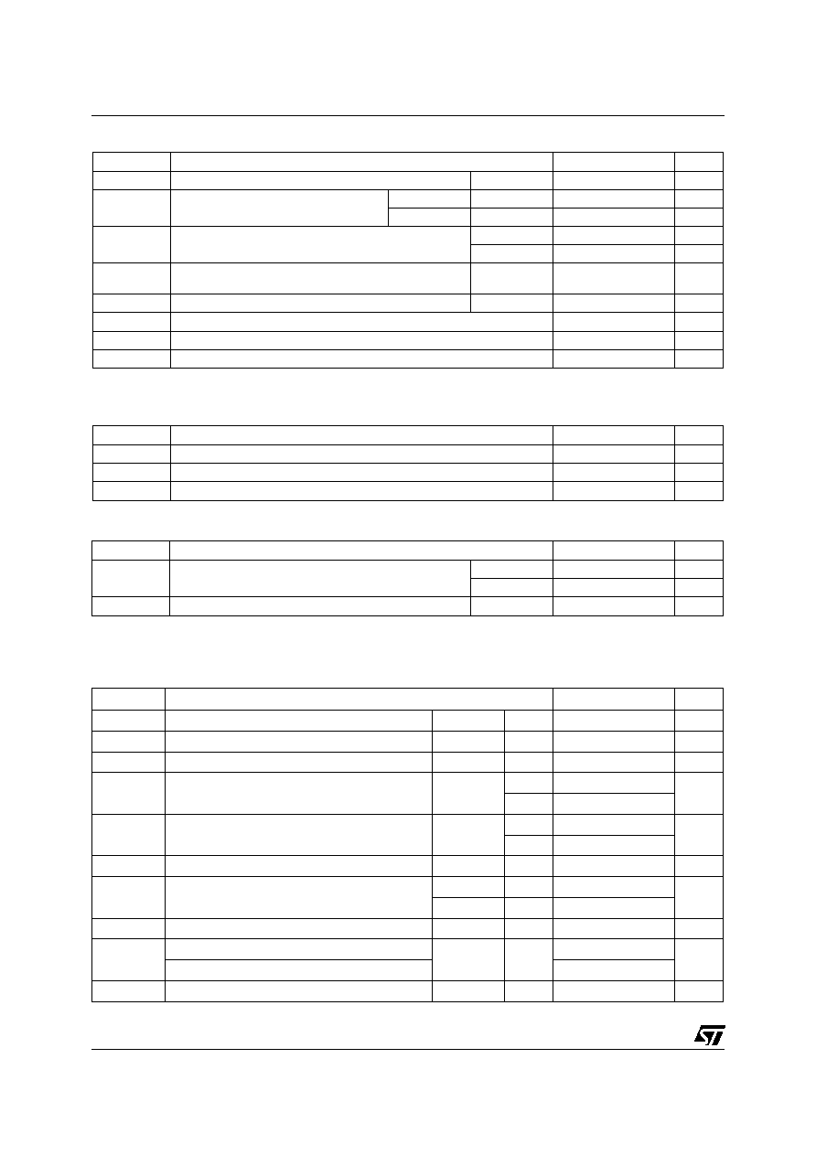
DESCRIPTION
OUT
COM
G
n
Needs no more external protection snubber or
varistor
n
Enables equipment to meet IEC 1000-4-5 &
IEC 335-1
n
Reduces component count by up to 80 %
n
Interfaces directly with a microcontroller
n
Eliminates any stressing gate kick back on
microcontroller
n
Allows straightforward connection of several
ACS on same cooling pad
BENEFITS
G
COM
OUT
ON
S
D
ACS102
FUNCTIONAL DIAGRAM
ASDTM
AC Switch Family
SO-8
ACS102-5T1
NC
NC
COM
COM
G
NC
NC
OUT
n
AC on-off static switching in appliance control
systems
n
Drive of low power high inductive or resistive
loads like
- relay, valve, solenoid, dispenser
- pump, fan, micro-motor
- low power lamp bulb, door lock
MAIN APPLICATIONS
NC: Not Connected
ACS102-5Tx
2/8
Symbol
Parameter
Value
Unit
V
DRM
/ V
RRM
Repetitive peak off-state voltage
Tj = 25 ∞C
500
V
I
T(RMS)
RMS on-state current full cycle sine
wave 50 to 60 Hz
TO92
Tamb = 75 ∞C
0.2
A
SO-8
Tamb = 75 ∞C
0.2
A
I
TSM
Non repetitive surge peak on-state current
Tj initial = 25∞C, full cycle sine wave
F =50 Hz
7.3
A
F =60 Hz
8
A
dI/dt
Critical rate of rise of on-state current
I
G
= 10mA, tr = 100ns
F =120 Hz
20
A/
µ
s
V
PP
Non repetitive line peak pulse voltage
note 1
2
kV
Tstg
Storage temperature range
- 40 to + 150
∞C
Tj
Operating junction temperature range
0 to + 110
∞C
Tl
Maximum lead temperature for soldering during 10s
260
∞C
note 1 : according to test described by IEC 1000-4-5 standard & Figure 4.
ABSOLUTE RATINGS (limiting values)
Symbol
Parameter
Value
Unit
P
G (AV)
Average gate power dissipation
0.1
W
I
GM
Peak gate current (tp = 20
µ
s)
1
A
V
GM
Peak positive gate voltage (respect to the pin COM)
5
V
SWITCH GATE CHARACTERISTICS (maximum values)
Symbol
Parameter
Value
Unit
Rth (j-a)
Junction to ambient
TO92
150
∞C/W
SO-8
150
∞C/W
Rth (j-l)
Junction to leads for full AC line cycle conduction
TO92
60
∞C/W
THERMAL RESISTANCES
Symbol
Test Conditions
Values
Unit
I
GT
V
OUT
=12V
(DC) R
L
=140
Tj=25∞C
MAX
5
mA
V
GT
V
OUT
=12V
(DC) R
L
=140
Tj=25∞C
MAX
0.9
V
V
GD
V
OUT
=V
DRM
R
L
=3.3k
Tj=110∞C
MIN
0.2
V
I
H
I
OUT
= 100mA gate open
Tj=25∞C
TYP
20
mA
MAX
tbd
I
L
I
G
= 20mA
Tj=25∞C
TYP
25
mA
MAX
tbd
V
TM
I
OUT
= 0.3A
tp=380
µ
s
Tj=25∞C
MAX
1.2
V
I
DRM
I
RRM
V
OUT
= V
DRM
V
OUT
= V
RRM
Tj=25∞C
MAX
2
µ
A
Tj=110∞C
MAX
50
dV/dt
V
OUT
=400V gate open
Tj=110∞C
MIN
300
V/
µ
s
(dI/dt)c
Turn off = 10ms, (dV/dt)c = 5V/
µ
s
Tj=110∞C
MIN
0.1
A/ms
Turn off = 20ms, (dV/dt)c = 10V/
µ
s
0.15
V
CL
I
CL
= 1mA
tp=1ms
Tj=25∞C
TYP
600
V
tbd = to be defined
ELECTRICAL CHARACTERISTICS
For either positive or negative polarity of pin OUT voltage respect to pin COM voltage
ACS102-5Tx
3/8
Parameter Symbol
Parameter Description
I
GT
Gate triggering current
V
GT
Gate triggering voltage
V
GD
Non triggering voltage
I
H
Holding current
I
L
Latching current
V
TM
On state voltage
I
DRM
/ I
RRM
Forward or reverse leakage current
dV/dt
Static pin OUT voltage rise
(dl/dt)
C
Turn off current rate of decay
V
CL
Clamping voltage
PARAMETER DESCRIPTION
The ACS102 device is well adapted to washing machine, dish washer, tumble drier, refrigerator, water
heaters, and cookware. It has been designed especially to switch on & off low power loads such as sole-
noid, valve, relay, dispenser, micro-motor, pump, fan, door lock, and low wattage lamps bulbs.
Pin COM
: Common drive reference to connect to the power line neutral
Pin G
: Switch Gate input to connect to the digital controller through a resistor
Pin OUT
: Switch Output to connect to the load
This ACS switch is triggered with a negative gate current flowing out of the gate pin G. It can be driven di-
rectly by the digital controller through a resistor as shown on the typical application diagram. No protection
device (zener or capacitor) are required between gate and COM terminals.
The SO-8 version allows to connect several ACS102 devices on the same cooling PCB pad which is the
COM pin.
In appliances systems, the ACS102 switch intends to drive low power load in full cycle ON / OFF mode.
The turn off commutation characteristics of these loads are described in table 1.
Thanks to its thermal and turn off commutation performances, the ACS102 switch is able to drive with no
turn off aid snubber a load up to 0.2 A (door lock, lamp, relay, valve & micro motor) when this load has to
switch off within one half AC line cycle, and up to 0.3 A (pump, fan) when this load can switch off within one
full AC line cycle.
AC LINE SWITCH BASIC APPLICATION
LOAD
IRMS
(A)
POWER
FACTOR
(dI/dt)c
(A/ms)
(dV/dt)c
(V/
µ
s)
TURN-OFF
DELAY
(ms)
Door lock, lamp
< 0.2
1
< 0.1
< 0.15
< 10
Relay Valve
Dispenser
Micro-motor
< 0.2
> 0.7
< 0.1
< 5
< 10
Pump Fan
< 0.3
> 0.2
< 0.15
< 10
< 20
Table 1: Low power load turn off commutation requirement (230V AC applications).
ACS102-5Tx
4/8
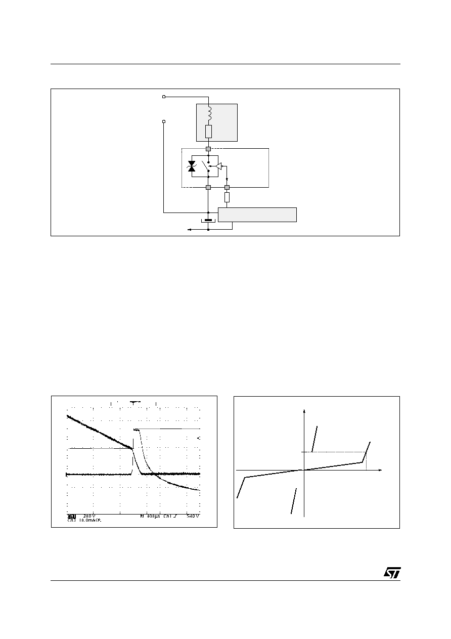
AC
MAINS
L
N
ST 72 MCU
LOAD
- Vcc
L
R
G
COM
OUT
ACS102
ON
S
D
TYPICAL APPLICATION DIAGRAM
At the end of the last conduction half-cycle, the load current reaches the holding current level I
H
, and the
ACSTM switch turns off. Because of the inductance L of the load, the current flows through the avalanche
diode D and decreases linearly to zero. During this time, the voltage across the switch is limited to the
clamping voltage V
CL
.
The energy stored in the inductance of the load depends on the holding current I
H
and the inductance (up
to 10 H); it can reach about 20 mJ and is dissipated in the clamping diode section. The ACS switch sustains
the turn off energy , because its clamping section is designed for that purpose.
HIGH INDUCTIVE SWITCH-OFF OPERATION
T
ime (400µs/div)
I
OUT
(10 mA/div)
V
OUT
(200V/div)
I
H
V
CL
= 650V
Fig 1: Turn-off operation of the ACS102 switch
with an electro valve: waveform of the gate current
I
G
, pin OUT current I
OUT
& voltage V
OUT
.
I
H
V
CL
I
OUT
V
OUT
Fig 2: ACS102 switch static characteristic.
ACS102-5Tx
5/8
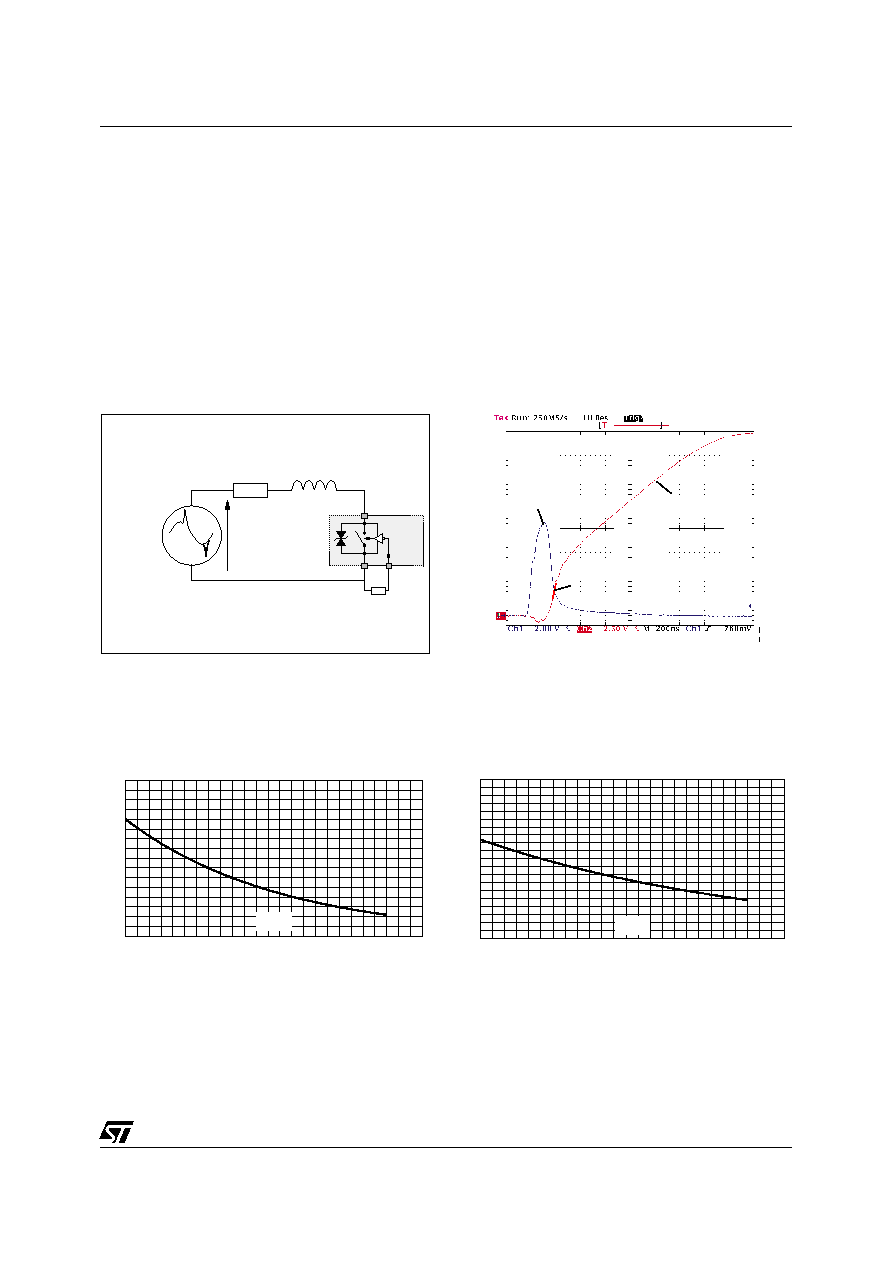
R
L
R
G
= 220
V
AC
+ V
PP
AC LINE &
SURGE VOLTAGE
GENERATOR
G
COM
OUT
ACSxx
ON
S
D
Fig. 3: Overvoltage ruggedness test circuit for
resistive and inductive loads according to
IEC 1000-4-5 standard.
R = 150
, L = 5
µ
H, V
PP
= 2kV.
The ACS102 switch is able to sustain safely the AC line transient voltages either by clamping the low en-
ergy spikes or by breaking over under high energy shocks, even with high turn-on current rates of increase.
The test circuit of the figure 3 is representative of the final ACS application and is also used to stress the
ACS switch according to the IEC1000-4-5 standard conditions. Thanks to the load, the ACS switch sus-
tains the voltage spikes up to 2 kV above the peak line voltage. It will breaks over safely even on resistive
load where the turn on current rate of increase is high as shown on figure 4. Such non repetitive test can be
done 10 times on each AC line voltage polarity.
AC LINE TRANSIENT VOLTAGE RUGGEDNESS
Vout (200 V/div)
Iout (2.5 A/div)
dI/dt = 70 A/µs
Fig. 4: Current and Voltage of the ACS during
IEC 1000-4-5 standard test with R = 150
, L =
5
µ
H & V
PP
= 2kV.
0
25
50
75
100
125
0.00
0.25
0.50
0.75
1.00
1.25
1.50
1.75
2.00
IGT[Tj]/IGT[Tj=25∞C]
Tj(∞C)
Fig 5: Relative variation of gate trigger current
versus junction temperature
0
25
50
75
100
125
0.0
0.2
0.4
0.6
0.8
1.0
1.2
1.4
1.6
1.8
2.0
IH[Tj]/IH[Tj=25∞C] & IL[Tj]/IL[Tj=25∞C]
Tj(∞C)
Fig 6:
Relative variation of holding & latching
currents versus junction temperature