Rev 1
January 2006
1/11
11
ACS102-6T
AC switch family
Transient protected AC switch (ACSTM)
Main product characteristics
Overvoltage protection by crowbar technology
High noise immunity - static dV/dt > 300 V/µs
Applications
AC ON/OFF static switching in appliances and
industrial control systems
Drive of low power high inductive or resistive
loads like:
≠ relay, valve, solenoid,
≠ dispenser, door lock
≠ micro-motor
Benefits
Needs no external protection snubber or
varistor.
Enables equipment to meet IEC 61000-4-5.
Reduces component count by up to 80%.
Interfaces directly with the micro-controller.
Common package tab connection supports
connection of several alternating current
switches (ACS) on the same cooling pad.
Integrated structure based on ASD
(1)
technology
Order code
Description
The ACS102-6T belongs to the AC line switch
family. This high performance switch can control a
load of up to 0.2A.
The ACS102-6T switch includes an overvoltage
crowbar structure to absorb the overvoltage
energy, and a gate level shifter driver to separate
the digital controller from the main switch. It is
triggered with a negative gate current flowing out
of the gate pin.
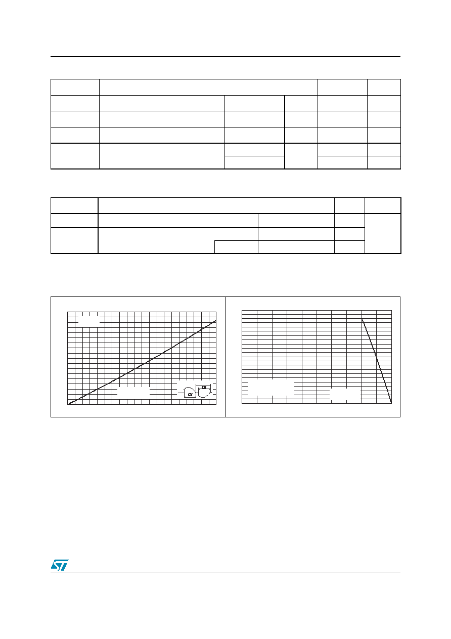
Functional diagram
TM: ACS is a trademark of STMicroelectronics
I
T(RMS)
0.2 A
V
DRM
/V
RRM
600 V
I
GT
5 mA
1.
ASD: Application Specific Devices
Part number
Marking
ACS102-6TA
ACS1026T
ACS102-6TA-TR
ACS1026T
ACS102-6T1
ACS1026T
ACS102-6T1-TR
ACS1026T
COM
Common drive reference to connect to the
mains
OUT
Output to connect to the load.
G
Gate input to connect to the controller through
gate resistor
COM
NC
NC
OUT
NC
NC
COM
G
COM
OUT
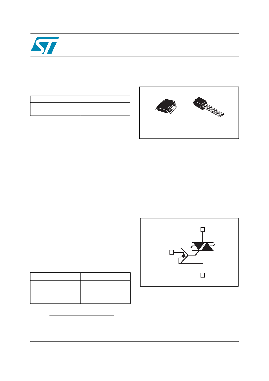
G
SO-8
ACS102-6T1
TO-92
ACS102-6TA
OUT
COM
G
www.st.com

1 Characteristics
ACS102-6T
2/11
1 Characteristics
Table 1.
Absolute maximum ratings (T
amb
= 25 ∞C, unless otherwise specified)
Table 2.
Electrical characteristics (T
j
= 25 ∞C, unless otherwise specified)
Symbol
Parameter
Value
Unit
I
T(RMS)
RMS on-state current (full sine wave)
TO-92
T
amb
= 100 ∞C
0.2
A
SO-08
T
amb
= 100 ∞C
I
TSM
Non repetitive surge peak on-state current
(full cycle sine wave, T
j
initial = 25 ∞C)
f = 60 Hz
t = 16.7 ms
7.6
A
f = 50 Hz
t = 20 ms
7.3
I≤t
I≤t Value for fusing
t
p
= 10 ms
0.38
A≤s
dI/dt
Critical rate of rise of on-state current
I
G
= 2xI
GT
, tr
100 ns
f = 120 Hz
T
j
= 125 ∞C
50
A/µs
V
PP
Non repetitive line peak mains voltage
(1)
1.
according to test described by IEC 61000-4-5 standard and
Figure 16
T
j
= 25 ∞C
2
kV
I
GM
Peak gate current
t
p
= 20 µs
T
j
= 125 ∞C
1
A
V
GM
Peak positive gate voltage
T
j
= 125 ∞C
10
V
P
G(AV)
Average gate power dissipation
T
j
= 125 ∞C
0.1
W
T
stg
T
j
Storage junction temperature range
Operating junction temperature range
-40 to +150
-30 to +125
∞C
Symbol
Test conditions
Quadrant
Value
Unit
I
GT
(1)
1.
minimum I
GT
is guaranteed at 10% of I
GT
max
V
OUT
= 12 V, R
L
= 33
II - III
MAX
5
mA
V
GT
II - III
MAX
0.9
V
V
GD
V
OUT
= V
DRM
, R
L
=3.3 k
, T
j
= 125 ∞C
II - III
MIN
0.15
V
I
H
(2)
2.
for both polarities of OUT referenced to COM
I
OUT
= 100 mA
MAX
20
mA
I
L
(2)
I
G
= 1.2 x I
GT
MAX
25
mA
dV/dt
(2)
V
OUT
= 67% V
DRM
,
gate open, T
j
= 125 ∞C
MIN
300
V/µs
(dI/dt)c
(2)
Without snubber (15 V/µs), turn-off time
20 ms, T
j
= 125 ∞C
MIN
0.15
A/ms
V
CL
I
CL
= 0.1 mA, t
p
= 1 ms, T
j
= 125 ∞C
MIN
650
V
ACS102-6T
1 Characteristics
3/11
Table 3.
Static electrical characteristics
Table 4.
Thermal resistance
Symbol
Test conditions
Value
Unit
V
TM
(1)
1.
for both polarities of OUT referenced to COM
I
TM
= 0.3 A, t
p
= 380 µs
Tj = 25 ∞C
MAX
1.2
V
V
TO
(1)
Tj = 125 ∞C
MAX
0.80
V
R
D
(1)
Tj = 125 ∞C
MAX
500
m
I
DRM
I
RRM
V
OUT
= 600 V
Tj = 25 ∞C
MAX
2
µA
Tj = 125 ∞C
0.2
mA
Symbol
Parameter
Value
Unit
R
th (j-l)
Junction to lead (AC)
TO-92
60
∞C/W
R
th (j-a)
Junction to ambient
TO-92
150
S = 40 mm≤
SO-8
150
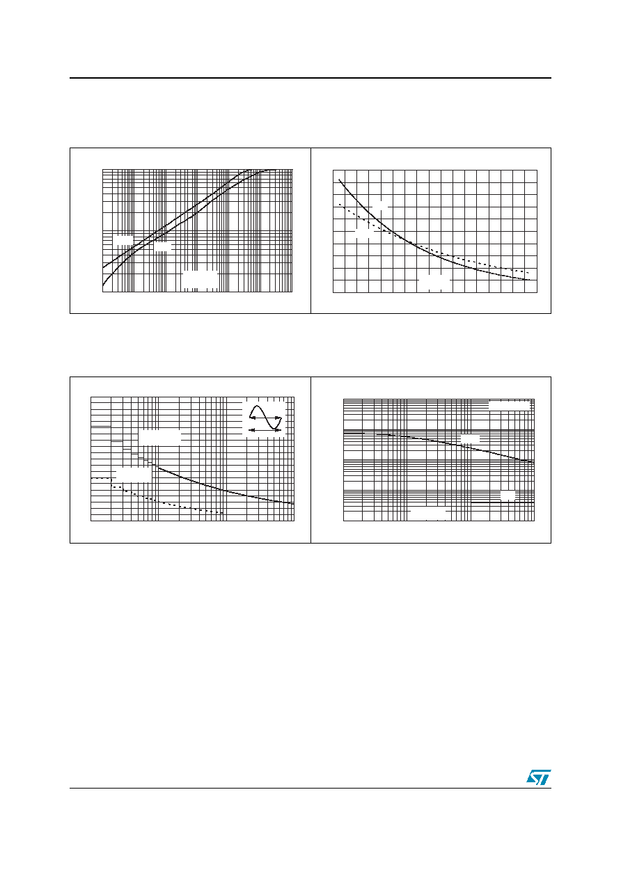
Figure 1.
Maximum power dissipation vs RMS
on-state current (full cycle)
Figure 2.
RMS on-state current vs ambient
temperature (full cycle)
0.00
0.02
0.04
0.06
0.08
0.10
0.12
0.14
0.16
0.18
0.00
0.02
0.04
0.06
0.08
0.10
0.12
0.14
0.16
0.18
0.20
P (W)
I
(A)
T(RMS)
=180∞
180∞
I
(A)
T(RMS)
0.00
0.02
0.04
0.06
0.08
0.10
0.12
0.14
0.16
0.18
0.20
0.22
0
25
50
75
100
125
a=180∞
Printed circuit board FR4
Natural convection
T
∞C
amb
1 Characteristics
ACS102-6T
4/11
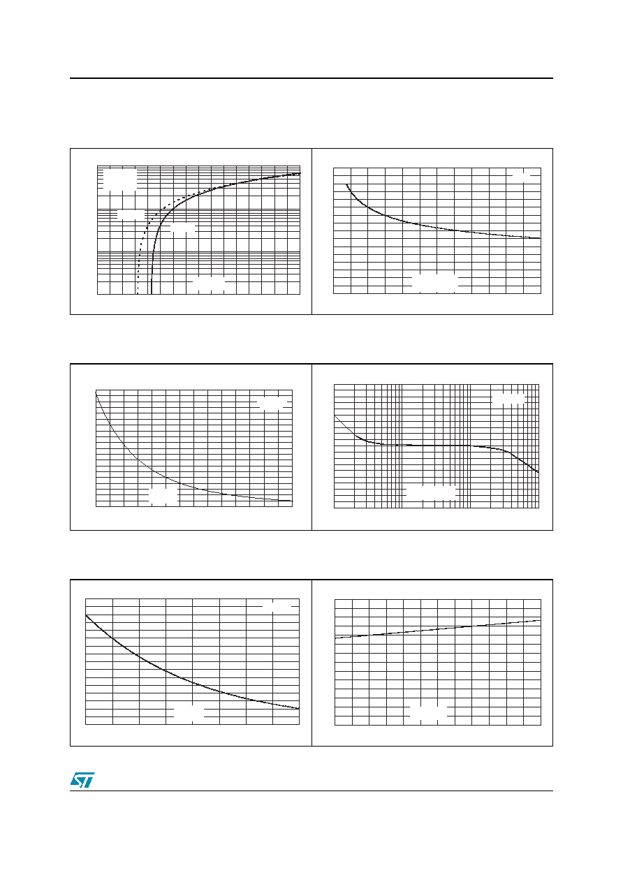
Figure 3.
Relative variation of junction to
ambient thermal impedance vs
pulse duration and package
Figure 4.
Relative variation of gate trigger
current, holding current and
latching current vs junction
temperature
Figure 5.
Non repetitive surge peak on-state
current vs number of cycles
Figure 6.
Non repetitive surge peak on-state
current for a sinusoidal pulse with
width tp<10 ms, and corresponding
value of I≤t (T
j
initial = 25 ∞C).
1.E-02
1.E-01
1.E+00
1.E-03
1.E-02
1.E-01
1.E+00
1.E+01
1.E+02
1.E+03
K=[Z
th(j-a)
/R
th(j-a)
]
TO-92
t (S)
P
SO-8
0.0
0.5
1.0
1.5
2.0
2.5
-40 -30 -20 -10
0
10 20 30 40 50 60 70 80 90 100 110 120 130
I
GT
, I
H
, I
L
[T
j
] / I
GT
, I
H
, I
L
[T
j
=25∞C]
T
j
(∞C)
I
L
& I
H
I
GT
0
1
2
3
4
5
6
7
8
9
10
1
10
100
1000
Number of cycles
I
TSM
(A)
Non repetitive
Tj initial=25∞C
Repetitive
T
amb
=100∞C
One cycle
t=20ms
1.E-01
1.E+00
1.E+01
1.E+02
1.E+03
0.01
0.10
1.00
10.00
I
TSM
(A), I≤t (A≤s)
Tj initial=25∞C
I
TSM
I≤t
(ms)
t
p
ACS102-6T
1 Characteristics
5/11
Figure 7.
On-state characteristics (maximal
values)
Figure 8.
SO-8 junction to ambient thermal
resistance versus copper surface
under tab (PCB FR4, copper
thickness 35 µm)
Figure 9.
Relative variation of critical rate of
decrease of main current (di/dt)c
versus junction temperature
Figure 10. Relative variation of critical rate of
decrease of main current (di/dt)c vs
(dV/dt)c, with turn-off time < 20 ms
Figure 11. Relative variation of static dV/dt
versus junction temperature
Figure 12. Relative variation of the maximal
clamping voltage versus junction
temperature (min value)
0.01
0.10
1.00
10.00
0.0
0.5
1.0
1.5
2.0
2.5
3.0
3.5
4.0
I
TM
(A)
T
j
max.:
V
to
= 0.8 V
R
d
= 500 m
Tj=25∞C
Tj=125∞C
V
TM
(V)
0
20
40
60
80
100
120
140
160
0
50
100
150
200
250
300
R
th(j-a)
(∞C/W)
SO-8
S
CU
(mm≤)
(dI/dt) [T ] / (dI/dt) [T =125 ∞C]
c
c
j
j
0
2
4
6
8
10
12
14
16
18
20
55
65
75
85
95
105
115
125
T (∞C)
j
V
out
= 400 V
(dI/dt)
c
[ (dV/dt)
c
] / Specified (dI/dt)
c
0.0
0.2
0.4
0.6
0.8
1.0
1.2
1.4
1.6
1.8
2.0
0.1
1
10
100
(dV/dt)
c
(V/µs)
V
out
= 400 V
0
1
2
3
4
5
6
7
8
25
50
75
100
125
dV/dt [T
j
] / dV/dt [T
j
=125∞C]
V
out
=400V
T
j
(∞C)
0.50
0.60
0.70
0.80
0.90
1.00
1.10
1.20
-25
0
25
50
75
100
125
V
CL
[T
j
] / V
DRM
T
j
(∞C)