
1/10
ACS110-7SN/SB2
Æ
April 2003 - Ed: 2A
AC LINE SWITCH
SOT-223
ACS110-7SN
s
Blocking voltage : V
DRM
/ V
RRM
= +/-700V
s
Avalanche controlled : V
CL
typ = 1100 V
s
Nominal conducting current : I
T(RMS)
= 1A
s
Gate triggering current : I
GT
< 10 mA
s
Switch integrated driver
s
High noise immunity : static dV/dt >500V/µs
FEATURES
The ACS110 belongs to the AC line switch family
built around the ASDTM concept. This high perfor-
mance switch circuit is able to control a load up to 1
A.
The ACSTM switch embeds a high voltage clamp-
ing structure to absorb the inductive turn off energy
and a gate level shifter driver to separate the digital
controller from the main switch. It is triggered with
a negative gate current flowing out of the gate pin.
DESCRIPTION
COM
COM
G
OUT
s
No external protection snubber or varistor
needed
s
Enables equipment to meet IEC 61000-4-5 &
IEC 335-1 (DIL-8 package)
s
Reduces component count up to 80 %
s
Interfaces directly with the microcontroller
s
Eliminates
any
gate
kick
back
on
the
microcontroller
s
Allows straightforward connection of several
ACSTM on same cooling pad (SOT-223)
BENEFITS
OUT
COM
G
S
D
ON
FUNCTIONAL DIAGRAM
ASDTM
AC Switch Family
DIL-8
ACS110-7SB2
COM
OUT
COM
COM
COM
G
s
AC static switching in appliance control systems
s
Drive of low power high inductive or resistive
loads like
- relay, valve, solenoid, dispenser
- pump, fan, micro-motor
- defrost heater
MAIN APPLICATIONS

ACS110-7SN/SB2
2/10
Symbol
Parameter
Value
Unit
V
DRM
/ V
RRM
Repetitive peak off-state voltage
Tj = -10 ∞C
700
V
I
T(RMS)
RMS on-state current full cycle sine wave
50 to 60 Hz
SOT-223
Ttab = 105 ∞C
1
A
DIL-8
Tlead = 110 ∞C
I
TSM
Non repetitive surge peak on-state current
Tj initial = 25∞C, full cycle sine wave
F =50 Hz
8
A
F =60 Hz
11
A
I
2
t
Fusing capability
tp = 10ms
0.35
A≤s
dI/dt
Repetitive on-state current critical rate of
rise I
G
= 10mA (tr < 100ns)
Tj = 125∞C
F = 120 Hz
50
A/
µ
s
V
PP
Non repetitive line peak pulse voltage
note 1
2
kV
Tstg
Storage temperature range
- 40 to + 150
∞C
Tj
Operating junction temperature range
- 30 to + 125
∞C
Tl
Maximum lead soldering temperature during 10s
260
∞C
Note 1: according to test described by IEC61000-4-5 standard & Figure 3.
ABSOLUTE RATINGS (limiting values)
For either positive or negative polarity of pin OUT voltage in respect to pin COM voltage
Symbol
Parameter
Value
Unit
P
G (AV)
Average gate power dissipation
0.1
W
I
GM
Peak gate current (tp = 20µs)
1
A
V
GM
Peak positive gate voltage (in respect to pin COM)
5
V
GATE CHARACTERISTICS (maximum values)
Symbol
Parameter
Value
Unit
Rth (j-a)
Junction to ambient S = 5cm≤
SOT-223
60
∞C/W
DIL-8
60
∞C/W
Rth (j-l)
Junction to tab/lead for full cycle sine wave conduction
SOT-223
20
∞C/W
DIL-8
15
∞C/W
S = Copper surface under Tab
THERMAL RESISTANCES
ACS110-7SN/SB2
3/10
Symbol
Test Conditions
Values
Unit
I
GT
V
OUT
=12V (DC)
R
L
=140
QII - QIII
Tj=25∞C
MAX
10
mA
V
GT
V
OUT
=12V (DC)
R
L
=140
QII - QIII
Tj=25∞C
MAX
1
V
V
GD
V
OUT
=V
DRM
R
L
=3.3k
Tj=125∞C
MIN
0.15
V
I
H
I
OUT
= 100mA gate open
Tj=25∞C
MAX
45
mA
I
L
I
G
= 20mA
Tj=25∞C
MAX
65
mA
V
TM
I
OUT
= 1.4A
tp=380
µ
s
Tj=25∞C
MAX
1.3
V
V
TO
Tj=125∞C
MAX
0.8
V
Rd
Tj=125∞C
MAX
300
m
I
DRM
/
I
RRM
V
OUT
= 700V
Tj=25∞C
MAX
2
µ
A
Tj=125∞C
MAX
200
dV/dt
V
OUT
=460V gate open
Tj=110∞C
MIN
500
V/
µ
s
(dI/dt)c
(dV/dt)c = 20V/
µ
s
Tj=125∞C
MIN
0.5
A/ms
V
CL
I
CL
= 1mA
tp=1ms
Tj=25∞C
TYP
1100
V
ELECTRICAL CHARACTERISTICS
For either positive or negative polarity of pin OUT voltage respect to pin COM voltage excepted note 3*.
Parameter Symbol
Parameter description
I
GT
Triggering gate current
V
GT
Triggering gate voltage
V
GD
Non-triggering gate voltage
I
H
Holding current
I
L
Latching current
V
TM
Peak on-state voltage drop
V
TO
On state threshold voltage
Rd
On state dynamic resistance
I
DRM
/ I
RRM
Maximum forward or reverse leakage current
dV/dt
Critical rate of rise of off-state voltage
(dV/dt)c
Critical rate of rise of commutating off-state voltage
(dI/dt)c
Critical rate of decrease of commutating on-state current
V
CL
Clamping voltage
I
CL
Clamping current
PARAMETER DESCRIPTION

ACS110-7SN/SB2
4/10
The ACS110 device is well adapted to Washing machine, dishwasher, tumble drier, refrigerator, water
heaters,air-conditioning systems, microwave ovens and other cookware. It has been designed especially
to switch on & off low power loads such as solenoid, valve, relay, dispenser, micro-motor, pump, fan and
defrost heaters.
Pin COM: Common drive reference to connect to the power line neutral
Pin G: Switch Gate input to connect to the digital controller
Pin OUT: Switch Output to connect to the load
This ACSTM switch is triggered with a negative gate current flowing out of the gate pin G. It can be driven di-
rectly by the digital controller through a resistor as shown on the typical application diagram.
Several ACS110 devices can be connected on the same cooling PCB pad, which is the COM pin.
Thanks to its thermal and turn off commutation performances, the ACS110 switch is able to drive with no
turn off additional snubber an inductive load up to 1 A.
AC LINE SWITCH BASIC APPLICATION
OUT
ACS110
COM
G
S
D
ON
ST72 MCU
N
AC
MAINS
L
R
- Vcc
L
M
LOAD
TYPICAL APPLICATION DIAGRAM
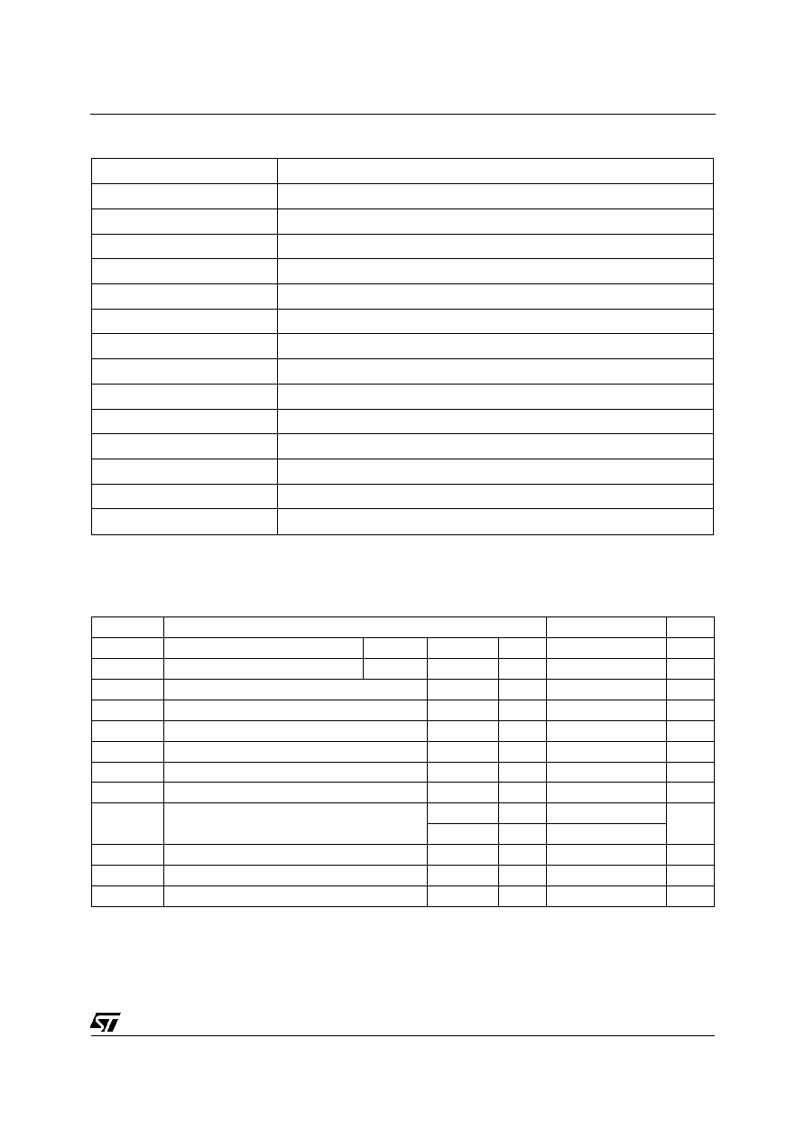
At the end of the last conduction half-cycle, the load current reaches the holding current level I
H
, and the
ACSTM switch turns off. Because of the inductance L of the load, the current flows then through the ava-
lanche diode D and decreases linearly to zero. During this time, the voltage across the switch is limited to
the clamping voltage V
CL
.
The energy stored in the inductance of the load depends on the holding current I
H
and the inductance (up
to 10 H); it can reach about 10 mJ and is dissipated in the clamping diode section. The ACS switch sustains
the turn off energy because its clamping section is designed for that purpose.
HIGH INDUCTIVE SWITCH-OFF OPERATION
ACS110-7SN/SB2
5/10
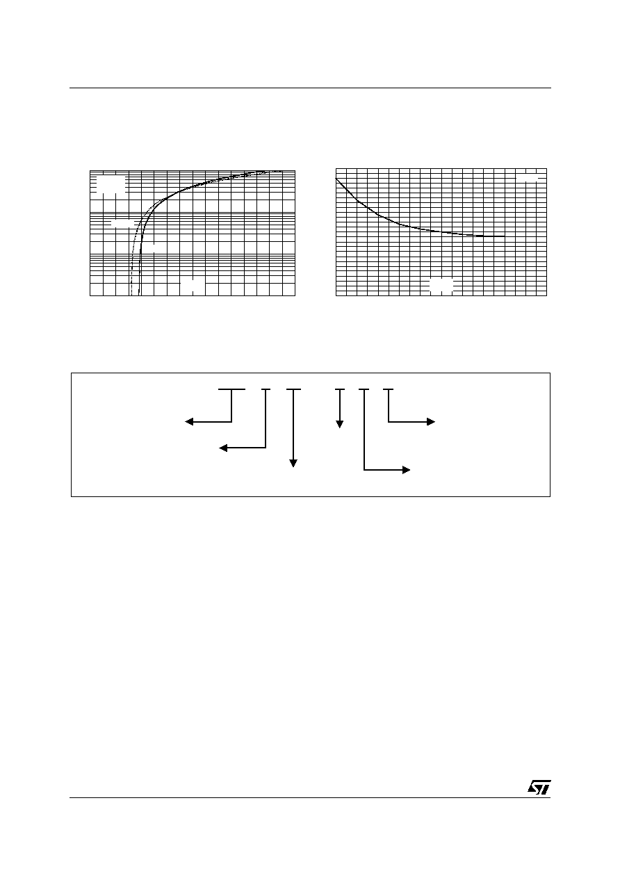
Fig. A: Turn-off operation of the ACS110 switch
with an electro-valve: waveform of the pin OUT
current I
OUT
and Out-COM voltage V
OUT
.
V
OUT
I
OUT
V
CL
I
H
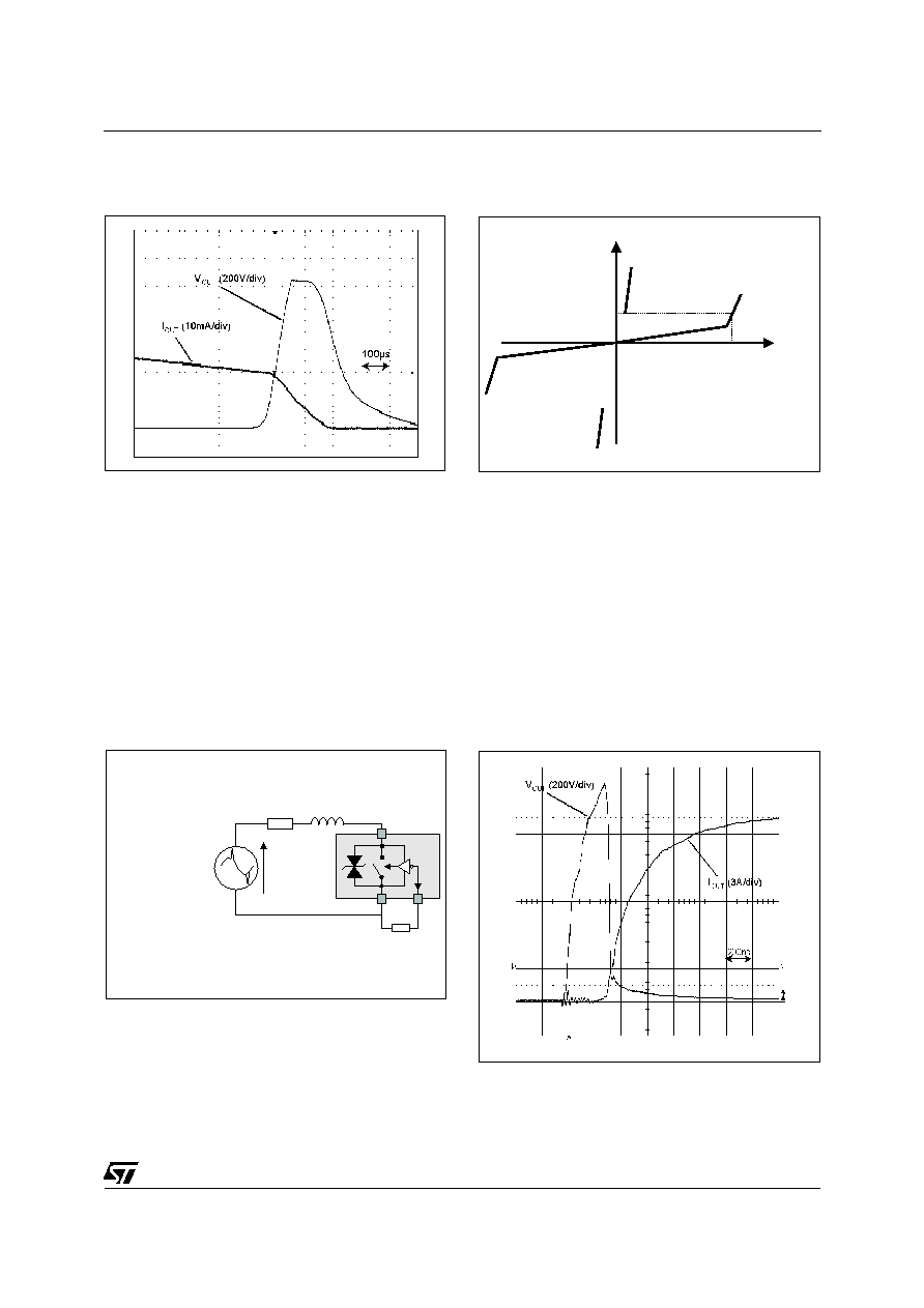
Fig. B: ACS110 switch static characteristic.
The ACS110 switch is able to sustain safely the AC line transient voltages either by clamping the low en-
ergy spikes or by breaking over under high energy shocks, even with high turn-on current rises.
The test circuit of the figure C is representative of the final ACS application and is also used to stress the
ACS switch according to the IEC 61000-4-5 standard conditions. Thanks to the load, the ACS switch sus-
tains the voltage spikes up to 2 kV above the peak line voltage. It will break over safely even on resistive
load where the turn on current rise is high as shown on figure D. Such non repetitive test can be done 10
times on each AC line voltage polarity.
AC LINE TRANSIENT VOLTAGE RUGGEDNESS
L
R
V
AC
+ V
PP
SURGE VOLTAGE
AC LINE & GENERATOR
RG = 220
COM
OUT
G
S
D
ON
ACSxx
Fig. C: Overvoltage ruggedness test circuit
for resistive and inductive loads according to
IEC61000-4-5 standards.
R = 150
, L = 10µH, V
PP
= 2kV.
Fig. D: Current and Voltage of the ACS110 dur-
ing IEC61000-4-5 standard test with R = 150
,
L = 10µH & V
PP
= 2kV.
ACS110-7SN/SB2
6/10
Maximum power dissipation vs RMS on state current.
RMS on-state current vs ambient temperature, case temperature and package
Relative variation of thermal impedance junction to ambient vs pulse duration and package
Relative variation of gate trigger current vs junction temperature
Relative variation of holding and latching current vs junction
Relative variation of dV/dt vs Tj
Relative variation of (dV/dt)
c
vs (di/dt)
c
Surge peak on-state current vs number of cycles
Non repetitive surge peak on-state current for a sinusoidal pulse with tp<10ms, and corresponding of I≤t.
On-state characteristics (maximal values)
Thermal resistance junction to ambient vs copper surface under tab
Relative variation of critical (di/dt)c vs junction temperature
OTHER FIGURES
0.0
0.1
0.2
0.3
0.4
0.5
0.6
0.7
0.8
0.9
1.0
1.1
0.0
0.1
0.2
0.3
0.4
0.5
0.6
0.7
0.8
0.9
1.0
I
(A)
T(RMS)
=180∞
180∞
P(W)
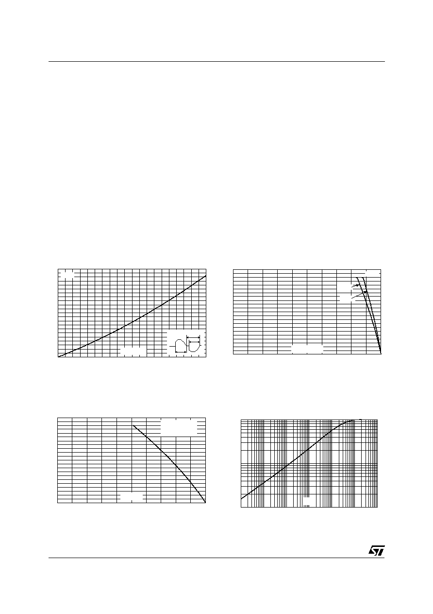
Fig. 1: Maximum power dissipation versus RMS
on-state current.
0.0
0.1
0.2
0.3
0.4
0.5
0.6
0.7
0.8
0.9
1.0
1.1
0
25
50
75
100
125
T
/T
(∞C)
tab
lead
=180∞
SOT-223
-
DIL-8
I
(A)
T(RMS)
Fig. 2-1: RMS on-state current versus tab or lead
temperature.
I
(A)
T(RMS)
0.0
0.1
0.2
0.3
0.4
0.5
0.6
0.7
0.8
0.9
1.0
1.1
0
25
50
75
100
125
T
(∞C)
amb
=180∞
Printed circuit board FR4
Natural convection
S=5cm≤
Fig. 2-2: RMS on-state current versus ambient
temperature.
1.E-02
1.E-01
1.E+00
1.E-03
1.E-02
1.E-01
1.E+00
1.E+01
1.E+02
1.E+03
t (s)
p
K=[Zth
/Rth
]
(j-a)
(j-a)
Fig. 3: Relative variation of thermal impedance
junction to ambient versus pulse duration.
ACS110-7SN/SB2
7/10
0.0
0.5
1.0
1.5
2.0
2.5
3.0
3.5
4.0
-40 -30 -20 -10
0
10
20
30
40
50
60
70
80
90 100 110 120 130
T (∞C)
j
I
GT
I & I
L
H
I
, I , I [T ] / I
, I , I [T = 25∞C]
GT
H
L
j
GT
H
L
j
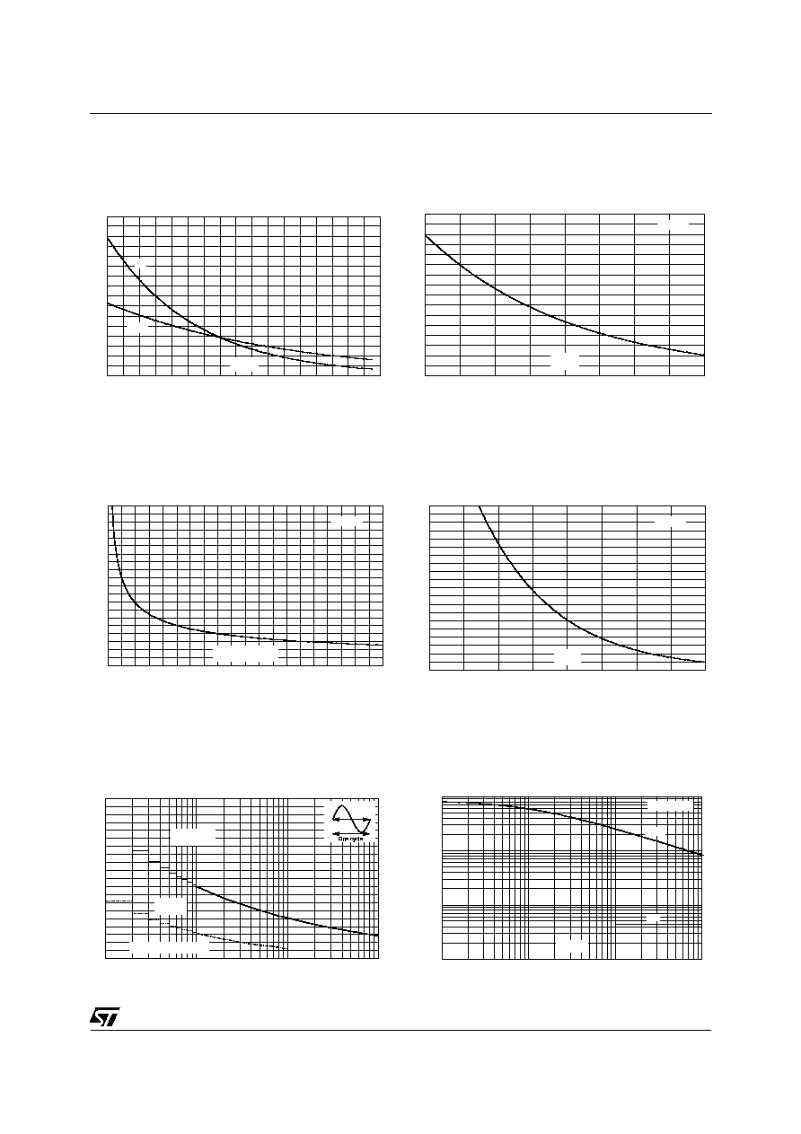
Fig. 4: Relative variation of gate trigger current,
holding current and latching versus junction
temperature (typical values).
0
1
2
3
4
5
6
7
8
25
50
75
100
125
T (∞C)
j
dV/dt [T ] / dV/dt [T = 125∞C]
j
j
V
OUT
=460V
Fig. 5: Relative variation of static dV/dt versus
junction temperature.
0
1
2
3
4
5
6
7
8
9
10
1
10
100
1000
Number of cycles
Non repetitive
T initial=25∞C
j
Repetitive
T =105∞C
ab
I
(A)
TSM
t=20ms
Fig. 8: Surge peak on-state current versus number
of cycles.
(dI/dt) [(dV/dt) ] / Specified (dI/dt)
c
c
c
0.0
0.5
1.0
1.5
2.0
2.5
3.0
3.5
4.0
4.5
5.0
0
5
10
15
20
25
30
35
40
45
50
(dV/dt) (V/µs)
c
V
OUT
=400V
Fig. 6: Relative variation of critical rate of de-
crease of main current versus reapplied dV/dt
(typical values).
0.1
1.0
10.0
100.0
0.01
0.10
1.00
10.00
t (ms)
p
I
TSM
I≤t
I
(A), I≤t (A≤s)
TSM
T initial=25∞C
j
Fig. 9: Non repetitive surge peak on-state current
for a sinusoidal pulse with width tp < 10ms, and
corresponding value of I≤t.
(dI/dt) [Tj] / (dI/dt) [T = 125∞C]
c
c
j
0
2
4
6
8
10
12
14
16
18
20
25
50
75
100
125
T (∞C)
j
V
OUT
=400V
Fig. 7: Relative variation of critical rate of decrease
of main current versus junction temperature.
ACS110-7SN/SB2
8/10
0
10
20
30
40
50
60
70
80
90
100
110
120
130
0.0
0.5
1.0
1.5
2.0
2.5
3.0
3.5
4.0
4.5
5.0
S(cm≤)
SOT-223
Rth
(∞C/W)
(j-a)
Fig. 11: Thermal resistance junction to ambient
versus copper surface under tab (printed circuit
board FR4, copper thickness: 35µm)
ACS 1 10 - 7 S X
AC Switch
Number of switches
I
10 = 1.0A
T(RMS)
V
7 = 700V
DRM
Gate Sensitivity
S= 10mA
Package
N = SOT-223
B2 = DIL-8
ORDERING INFORMATION
0.01
0.10
1.00
10.00
0.0
0.5
1.0
1.5
2.0
2.5
3.0
3.5
4.0
V
(V)
TM
T
j
max. :
V =0.8V
R =300m
to
d
T
j
=25∞C
T
j
=125∞C
I
(A)
TM
Fig.
10:
On-state
characteristics
(maximum
values).

ACS110-7SN/SB2
9/10
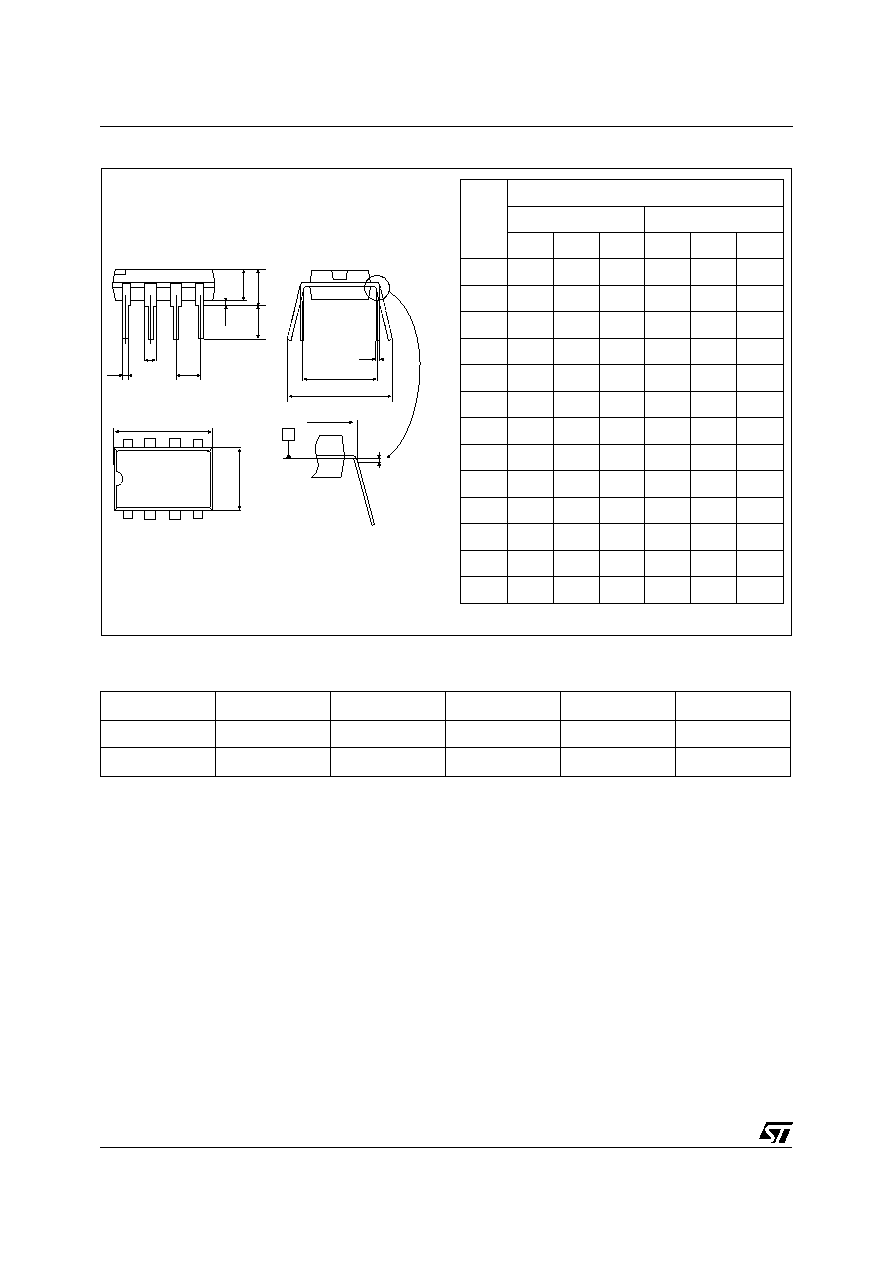
PACKAGE OUTLINE MECHANICAL DATA
SOT-223
REF.
DIMENSIONS
Millimeters
Inches
Min.
Typ.
Max.
Min.
Typ.
Max.
A
1.80
0.071
A1
0.02
0.10
0.001
0.004
B
0.60
0.70
0.85
0.024 0.027
0.033
B1
2.90
3.00
3.15
0.114 0.118
0.124
c
0.24
0.26
0.35
0.009 0.010
0.014
D
6.30
6.50
6.70
0.248 0.256
0.264
e
2.3
0.090
e1
4.6
0.181
E
3.30
3.50
3.70
0.130 0.138
0.146
H
6.70
7.00
7.30
0.264 0.276
0.287
V
10∞ max
A
A1
B
e1
D
B1
H
E
e
c
V
1
4
2
3
DESCRIPTION
PIN
1
2
3
4
GATE
DRAIN
SOURCE
DRAIN
BASE
COLLECTOR
COLLECTOR
EMITTER
Recommended soldering pattern SOT-223
PACKAGE FOOT PRINT
SOT-223
ACS110-7SN/SB2
10/10
Information furnished is believed to be accurate and reliable. However, STMicroelectronics assumes no responsibility for the consequences of
use of such information nor for any infringement of patents or other rights of third parties which may result from its use. No license is granted by
implication or otherwise under any patent or patent rights of STMicroelectronics. Specifications mentioned in this publication are subject to
change without notice. This publication supersedes and replaces all information previously supplied.
STMicroelectronics products are not authorized for use as critical components in life support devices or systems without express written ap-
proval of STMicroelectronics.
The ST logo is a registered trademark of STMicroelectronics
© 2003 STMicroelectronics - Printed in Italy - All rights reserved.
STMicroelectronics GROUP OF COMPANIES
Australia - Brazil - Canada - China - Finland - France - Germany
Hong Kong - India - Israel - Italy - Japan - Malaysia - Malta - Morocco - Singapore
Spain - Sweden - Switzerland - United Kingdom - United States.
http://www.st.com
PACKAGE OUTLINE MECHANICAL DATA
DIL-8
8
1
5
4
eB
E
H
GAUGE PLANE 0.38
D
E1
eA
c
b
b2
e
A
L
A1
A2
REF.
DIMENSIONS
Millimetres
Inches
Min.
Typ. Max.
Min.
Typ. Max.
A
5.33
0.21
A1
0.38
0.015
A2
2.92
3.30
4.95 0.115 0.130 0.195
b
0.36
0.46
0.56 0.014 0.018 0.022
b2
1.14
1.52
1.78 0.045 0.060 0.070
c
0.20
0.25
0.36 0.008 0.010 0.014
D
9.02
9.27 10.16 0.355 0.365 0.40
E
7.62
7.87
8.26
0.30 0.310 0.325
E1
6.10
6.35
7.11 0.240 0.25 0.280
e
2.54
0.10
eA
7.62
0.30
eB
10.92
0.430
L
2.92
3.30
3.81 0.115 0.130 0.15
Ordering type
Marking
Package
Weight
Base qty
Delivery mode
ACS110-7SN
ACS1107S
SOT-223
0.12 g
1000
Tape & reel
ACS110-7SB2
ACS1107S
DIL8
0.6 g
50
Tube
s
Epoxy meets UL94,V0
OTHER INFORMATION