 | –≠–ª–µ–∫—Ç—Ä–æ–Ω–Ω—ã–π –∫–æ–º–ø–æ–Ω–µ–Ω—Ç: ACST4-7CB | –°–∫–∞—á–∞—Ç—å:  PDF PDF  ZIP ZIP |
1/9
ACST4 Series
Æ
January 2003 - Ed: 3A
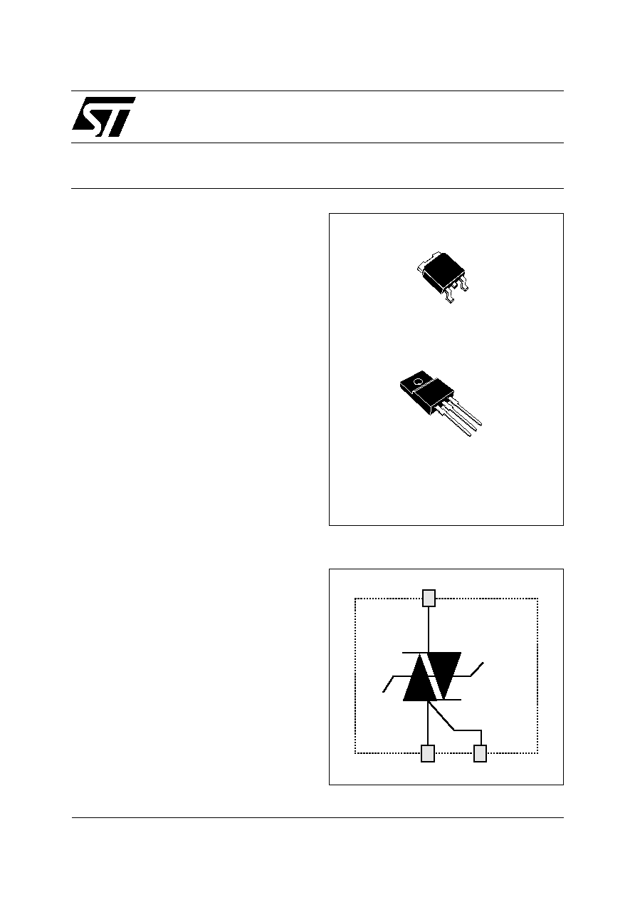
AC POWER SWITCH
DPAK
ACST4-7SB/CB
s
Blocking voltage : V
DRM
/ V
RRM
= +/-700V
s
Avalanche controlled : V
CL
typ = 1100 V
s
Nominal conducting current : I
T(RMS)
= 4A
s
High surge current capability: 30A for 20ms full
wave
s
Gate triggering current : I
GT
< 10 mA or 25mA
s
Switch integrated driver
s
High noise immunity : static dV/dt >500V/µs
FEATURES
The ACST4 belongs to the AC power switch family
built around the ASDTM technology. This high per-
formance device is adapted to home appliances or
inductrial systems and drives loads up to 4 A.
The ACSTM switch embeds a Triac structure with a
high voltage clamping device to absorb the induc-
tive turn-off energy and withstand line transients
such as those described in the IEC61000-4-5 stan-
dards.
DESCRIPTION
OUT
COM
G
s
Enables equipment to meet IEC 61000-4-5
s
High off-state reliability with planar technology
s
No external overvoltage protection needed
s
Reduces the power component factor
s
Interfaces directly with the microcontroller
s
Direct interface with the microcontroller for the
ACST4-7S (I
GT
< 10mA)
BENEFITS
OUT
COM
G
FUNCTIONAL DIAGRAM
ASDTM
AC Switch Family
TO-220FPAB
ACST4-7SFP/CFP
OUT
COM
G
s
AC static switching in appliance control systems
s
Drive of low power high inductive or resistive
loads like
- spray pump in dishwashers
- fan in air-conditioners
MAIN APPLICATIONS

ACST4 Series
2/9
Symbol
Parameter
Value
Unit
V
DRM
/ V
RRM
Repetitive peak off-state voltage
Tj = -10 ∞C
700
V
I
T(RMS)
RMS on-state current full cycle sine
wave 50 to 60 Hz
DPAK
Tc = 110 ∞C
4
A
TO-220FPAB
Tc = 100 ∞C
I
TSM
Non repetitive surge peak on-state current
Tj initial = 25∞C, full cycle sine wave
F =50 Hz
30
A
F =60 Hz
33
A
I
2
t
Fusing capability
tp = 10ms
6.4
A≤s
dI/dt
Repetitive on-state current critical rate
of rise I
G
= 10mA (tr < 100ns)
Tj = 125∞C
F = 120 Hz
50
A/
µ
s
V
PP
Non repetitive line peak pulse voltage
note 1
2
kV
Tstg
Storage temperature range
- 40 to + 150
∞C
Tj
Operating junction temperature range
- 30 to + 125
∞C
Tl
Maximum lead soldering temperature during 10s
260
∞C
Note 1: according to test described by IEC61000-4-5 standard & Figure B.
ABSOLUTE RATINGS (limiting values)
For either positive or negative polarity of pin OUT voltage in respect to pin COM voltage
Symbol
Parameter
Value
Unit
P
G (AV)
Average gate power dissipation
0.1
W
P
GM
Peak gate power dissipation (tp = 20µs)
10
A
I
GM
Peak gate current (tp = 20µs)
1
V
GATE CHARACTERISTICS (maximum values)
Symbol
Parameter
Value
Unit
Rth (j-a)
Junction to ambient
S = 0.5cm≤
DPAK
70
∞C/W
TO-220FPAB
60
∞C/W
Rth (j-l)
Junction to case for full cycle sine wave
conduction
DPAK
2.6
∞C/W
TO-220FPAB
4.6
∞C/W
S = Copper surface under Tab
THERMAL RESISTANCES

ACST4 Series
3/9
Symbol
Test Conditions
ACST4-7S
ACST4-7C
Unit
I
GT
V
OUT
=12V (DC)
R
L
=33
QI - QII - QIII
Tj=25∞C
MAX
10
25
mA
V
GT
V
OUT
=12V (DC)
R
L
=33
QI - QII - QIII
Tj=25∞C
MAX
1
1.1
V
V
GD
V
OUT
=V
DRM
R
L
=3.3k
Tj=125∞C
MIN
0.2
V
I
H
I
OUT
= 100mA gate open
Tj=25∞C
MAX
20
35
mA
I
L
I
G
= 2 x I
Gt
max
Tj=25∞C
MAX
40
60
mA
V
TM
I
OUT
= 5.6A
tp=380
µ
s
Tj=25∞C
MAX
1.5
V
V
TO
Tj=125∞C
MAX
0.90
V
Rd
Tj=125∞C
MAX
100
m
I
DRM
/
I
RRM
V
OUT
= 700V
Tj=25∞C
MAX
10
µ
A
Tj=125∞C
MAX
500
dV/dt
V
OUT
=460V gate open
Tj=110∞C
MIN
200
500
V/
µ
s
(dI/dt)c
(dV/dt)c = 15V/
µ
s
Tj=125∞C
MIN
2.0
2.5
A/ms
V
CL
I
CL
= 1mA
tp=1ms
Tj=25∞C
TYP
1100
V
ELECTRICAL CHARACTERISTICS
For either positive or negative polarity of pin OUT voltage in respect to pin COM voltage.
Parameter Symbol
Parameter description
I
GT
Triggering gate current
V
GT
Triggering gate voltage
V
GD
Non-triggering gate voltage
I
H
Holding current
I
L
Latching current
V
TM
Peak on-state voltage drop
V
TO
On state threshold voltage
Rd
On state dynamic resistance
I
DRM
/ I
RRM
Maximum forward or reverse leakage current
dV/dt
Critical rate of rise of off-state voltage
(dV/dt)c
Critical rate of rise of commutating off-state voltage
(dI/dt)c
Critical rate of decrease of commutating on-state current
V
CL
Clamping voltage
I
CL
Clamping current
PARAMETER DESCRIPTION

ACST4 Series
4/9
The ACST4 device has been designed to switch on & off low power, but highly inductive or resistive loads
such as dishwashers spray pumps, and air-conditioners fan.
Pin COM: Common drive reference to connect to the power line neutral
Pin G: Switch Gate input to connect to the digital controller
Pin OUT: Switch Output to connect to the load
ACST4-7S triggering current has to be sunk from the gate pin G. The switch can then be driven directly by
logic level circuits through a resistor as shown on the typical application diagram ( Fig A ).
Thanks to its thermal and turn off commutation performances, the ACST4 switch is able to drive with no
turn off additional snubber an inductive load up to 4 A.
AC LINE SWITCH BASIC APPLICATION
OUT
COM
G
ACST4
ST72 MCU
N
AC
MAINS
L
R
- Vcc
M
LOAD
OUT
L
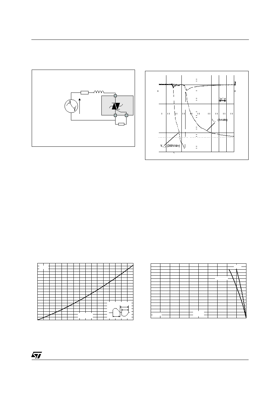
TYPICAL APPLICATION DIAGRAM (Fig. A)
The ACST4 switch is able to sustain safely the AC line transient voltages either by clamping the low energy
spikes or by breaking over under high energy shocks, even with high turn-on current rises.
The test circuit of the figure 2 is representative of the final ACST application and is also used to stress the
ACST switch according to the IEC 61000-4-5 standard conditions. Thanks to the load, the ACST switch
sustains the voltage spikes up to 2 kV above the peak line voltage. It will break over safely even on resistive
load where the turn on current rate of rise, is as high as shown on figure 3. Such non-repetitive test can be
done 10 times on each AC line voltage polarity.
AC LINE TRANSIENT VOLTAGE RUGGEDNESS
ACST4 Series
5/9
L
R
V
AC
+ V
PP
SURGE VOLTAGE
AC LINE & GENERATOR
RG = 220
COM
OUT
G
ACST4
Fig. B: Overvoltage ruggedness test circuit for re-
sistive
and
inductive
loads
according
to
IEC61000-4-5 standards.
R = 150
, L = 10µH, V
PP
= 2kV.
Fig. C: Current and Voltage of the ACST4 dur-
ing IEC61000-4-5 standard test with R, L & V
PP
.
0.0
0.5
1.0
1.5
2.0
2.5
3.0
3.5
4.0
4.5
5.0
0.0
0.5
1.0
1.5
2.0
2.5
3.0
3.5
4.0
I
(A)
T(RMS)
=180∞
P(W)
180∞
Fig. 1: Maximum power dissipation versus RMS
on-state current.
0.0
0.5
1.0
1.5
2.0
2.5
3.0
3.5
4.0
4.5
0
25
50
75
100
125
Tc(∞C)
=180∞
DPAK
TO-220FPAB
I
(A)
T(RMS)
Fig. 2-1:
RMS on-state current versus case
temperature.