 | –≠–ª–µ–∫—Ç—Ä–æ–Ω–Ω—ã–π –∫–æ–º–ø–æ–Ω–µ–Ω—Ç: ACST6-7SR | –°–∫–∞—á–∞—Ç—å:  PDF PDF  ZIP ZIP |
1/9
ACST6-7S
Æ
January 2002 - Ed: 7F
OVER VOLTAGE PROTECTED
AC POWER SWITCH
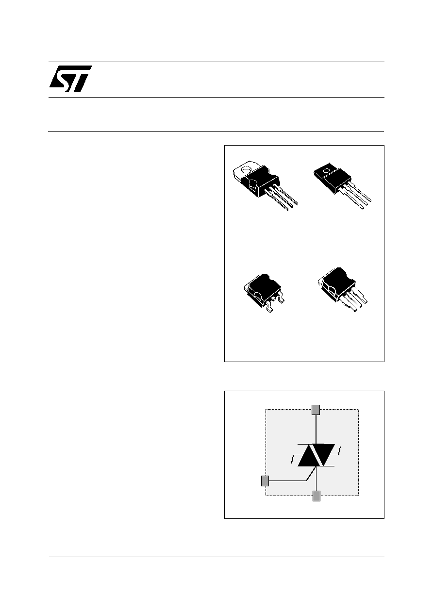
TO-220AB
ACST6-7ST
s
V
DRM
/ V
RRM
= +/- 700V
s
Avalanche controlled device
s
I
T(RMS)
=1.5 A with no heat sink and T
amb
= 40∞C
s
I
T(RMS)
= 6A with T
CASE
= 105 ∞C
s
High noise immunity: static dV/dt > 200 V/µs
s
Gate triggering current : I
GT
< 10 mA
s
Snubberless turn off commutation:
(dI/dt)c > 3.5A/ms
s
D
2
PAK, I
2
PAK, TO-220FPAB or TO-220
package
FEATURES
The ACST6-7Sx belongs to the AC power switch
family built around the ASD technology. This high
performance device is adapted to home appliances
or industrial systems and drives an induction motor
up to 6A.
This ACST switch embeds a triac structure with a
high voltage clamping device to absorb the inductive
turn-off energy and withstand line transients such as
those described in the IEC61000-4-5 standards.
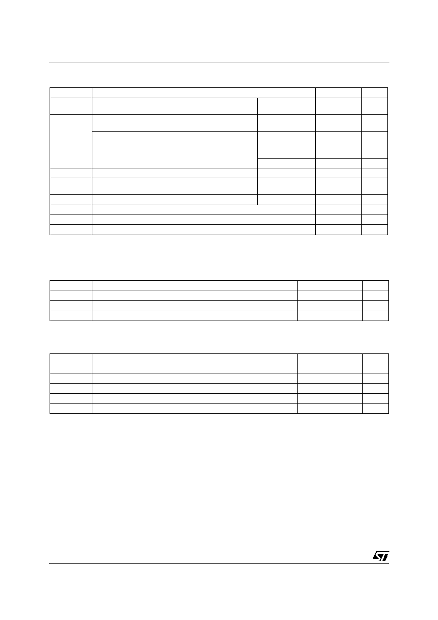
DESCRIPTION
COM
OUT
OUT
G
s
Enables equipment to meet IEC61000-4-5
standards
s
High off-state reliability with planar technology
s
Needs no external overvoltage protection
s
Direct interface with the microcontroller
s
Reduces the power component count
BENEFITS
G
COM
OUT
FUNCTIONAL DIAGRAM:
s
AC static switching in appliance & industrial
control systems
s
Induction motor drive actuator for:
- Refrigerator / Freezer compressor
- Dishwasher spray pump
- Clothes drier tumble
s
Actuator for the thermostat of a refrigerator or
freezer
MAIN APPLICATIONS
ASDTM
AC Switch Family
G
OUT
COM
D
2
PAK
ACST6-7SG
COM
G
OUT
TO-220FPAB
ACST6-7SFP
COM
OUT
G
OUT
I
2
PAK
ACST6-7SR
ACST6-7S
2/9
Symbol
Parameter
Value
Unit
V
DRM /
V
RRM
Repetitive peak off-state voltage
Tj = 125 ∞C
700
V
I
T(RMS)
RMS on-state current full cycle sine wave 50 to 60 Hz,
no heat sink
Tamb = 40 ∞C
1.5
A
RMS on-state current full cycle sine wave 50 to 60 Hz,
TO-220AB package
Tcase= 105 ∞C
6
A
I
TSM
Non repetitive surge peak on-state current
Tj initial = 25∞C, full cycle sine wave
tp = 20ms
45
A
tp = 16.7ms
50
A
I
2
t
Thermal constraint for fuse selection
tp = 10ms
11
A
2
s
dI/dt
Non repetitive on-state current critical rate of rise
I
G
= 10mA (t
R
< 100ns)
Rate period > 1mn
100
A/
µ
s
V
PP
Non repetitive line peak pulse voltage
note 1
2
kV
Tstg
Storage temperature range
- 40 to + 150
∞C
Tj
Operating junction temperature range
- 30 to + 125
∞C
Tl
Maximum lead soldering temperature during 10s
260
∞C
Note 1: according to test described by IEC61000-4-5 standard & Figure A.
ABSOLUTE RATINGS (limiting values)
Symbol
Parameter
Value
Unit
P
G (AV)
Average gate power dissipation
0.1
W
P
GM
Peak gate power dissipation (tp = 20µs)
10
W
I
GM
Peak gate current (tp = 20µs)
1
A
GATE CHARACTERISTICS (maximum values)
Symbol
Parameter
Value
Unit
Rth (j-a)
Junction to ambient TO-220AB / TO-220FPAB
60
∞
C/W
Rth (j-a)
Junction to ambient I
2
PAK
65
∞
C/W
Rth (j-a)
Junction to ambient D
2
PAK soldered on 1cm
2
copper pad
45
∞
C/W
Rth (j-c)
Junction to case for full cycle sine wave conduction (TO-220AB)
2.5
∞
C/W
Rth (j-c)
Junction to case for full cycle sine wave conduction (TO-220FPAB)
3.5
∞C/W
THERMAL RESISTANCE

ACST6-7S
3/9
Symbol
Test conditions
Values
Unit
I
GT
Vout = 12V (DC)
R
L
= 33
Tj = 25∞C
MAX.
10
mA
V
GT
Vout = 12V (DC)
R
L
= 33
Tj = 25∞C
MAX.
1.5
V
V
GD
V
OUT
= V
DRM
R
L
= 3.3k
Tj =125∞C
MIN.
0.2
V
I
H
I
OUT
= 100mA Gate open
Tj = 25∞C
MAX.
25
mA
I
L
I
G
= 20mA
Tj = 25∞C
MAX.
50
mA
V
TM
I
OUT
= 2.1A
tp = 380µs
Tj = 25∞C
MAX.
1.4
V
V
TM
I
OUT
= 8.5A
tp = 380µs
Tj = 25∞C
MAX.
1.7
V
V
to
Tj = 125∞C
MAX.
0.9
V
R
D
Tj = 125∞C
MAX.
80
m
I
DRM
I
RRM
V
OUT
= V
DRM
V
OUT
= V
RRM
Tj = 25∞C
MAX.
20
µ
A
Tj = 125∞C
MAX.
500
µ
A
dV/dt
V
OUT
= 600V
gate open
Tj = 125∞C
MIN.
200
V/
µ
s
(dI/dt)c
(dV/dt)c = 15V/
µ
s
Tj = 125∞C
MIN.
3
A/ms
(dI/dt)c
(dV/dt)c = 15V/
µ
s Iout < 0 Rgk = 150
Tj = 125∞C
MIN.
3.5
A/ms
V
CL
I
CL
= 1mA
tp = 1ms
Tj = 25∞C
TYP.
1100
V
ELECTRICAL CHARACTERISTICS PER SWITCH
For either positive or negative polary of pin OUT voltage in respect to pin COM voltage
Parameter Symbol
Parameter description
I
GT
Gate triggering current
V
GT
Gate triggering voltage
V
GD
Non triggering voltage
I
H
Holding current
I
L
Latching current
V
TM
On state voltage
V
TO
On state characteristic threshold voltage
R
D
On state characteristic dynamic resistance
I
DRM
/ I
RRM
Forward or reverse leakage current
dV/dt
Static pin OUT voltage rise
(dI/dt)c
Turn off current rate of decay
V
CL
Avalanche voltage at turn off
PARAMETER DESCRIPTION

ACST6-7S
4/9
ST 62/72
MCU
COM
OUT
G
Run
Start
ST 62/72
MCU
Run
Start
COM
OUT
G
TYPICAL APPLICATION DIAGRAM
The ACST6-7S device is especially designed to drive medium power induction motors in refrigerators, dish
washers, and tumble dryers.
Pin COM
: Common drive reference, to be connected to the power line neutral
Pin G
: Switch Gate input to be connected to the controller
Pin OUT
: Switch Output to be connected to the load
When driven from a low voltage controller, the ACST switch is triggered with a negative gate current flow-
ing out of the gate pin G. It can be directly driven by the controller through a resistor as shown on the typical
application diagram. In appliance systems, the ACST6-7S switch intends to drive medium power load in
ON / OFF full cycle or phase angle control mode.
Thanks to its thermal and turn-off commutation characteristics, the ACST6-7S switch is able to drive an
inductive load up to 6A without a turn-off aid snubber circuit.
AC LINE SWITCH BASIC APPLICATION
The ACST6-7S switch is able to safely withstand the AC line transient voltages either by clamping the low
energy spikes or by breaking over under high energy shocks.
The test circuit in Figure A is representative of the ACST application and is used to test the ACST switch
according to the IEC61000-4-5 standard conditions. Thanks to the load impedance, the ACST switch with-
stands voltage spikes up to 2 kV above the peak line voltage by breaking over safely. Such non-repetitive
testing can be done 10 times on each AC line voltage polarity.
AC LINE TRANSIENT VOLTAGE RUGGEDNESS
L
R
V
AC
+ V
PP
SURGE VOLTAGE
AC LINE & GENERATOR
G
COM
OUT
Fig. A: Overvoltage ruggedness test circuit for resistive and inductive loads according
to IEC61000-4-5 standard R = 10
, L = 5µH & V
PP
= 2kV
ACST6-7S
5/9
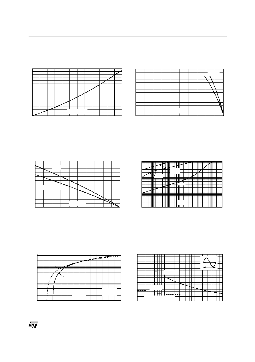
0
1
2
3
4
5
6
0
1
2
3
4
5
6
7
8
IT(RMS) (A)
P (W)
Fig. 1: Maximum power dissipation versus RMS
on-state current (full cycle).
0
25
50
75
100
125
0
1
2
3
4
5
6
7
Tc(∞C)
IT(RMS) (A)
TO-220AB
D≤PAK
TO-220FP
Fig. 2-1: RMS on-state current versus case
temperature (full cycle).
0
25
50
75
100
125
0.0
0.5
1.0
1.5
2.0
2.5
3.0
Tamb(∞C)
IT(RMS) (A)
D≤PAK
S=1cm≤
TO-220AB or TO-220FP
Free air
Fig. 2-2: RMS on-state current versus ambient
temperature (printed circuit board FR4, copper
thickness: 35µm), full cycle.
1E-3
1E-2
1E-1
1E+0
1E+1
1E+2 5E+2
1E-3
1E-2
1E-1
1E+0
tp (s)
K=[Zth/Rth]
Zth(j-a)
Zth(j-c)
TO-220AB
& D≤PAK
Zth(j-c)
TO-220FP
Fig. 3: Relative variation of thermal impedance
versus pulse duration.
0.5
1.0
1.5
2.0
2.5
3.0
3.5
4.0
0.1
1.0
10.0
50.0
VTM (V)
ITM (A)
Tj=25∞C
Tj max.
Tj max.:
Vto = 0.9 V
Rd = 80 mW
Fig. 4: On-state characteristics (maximum values).
1
10
100
1000
0
5
10
15
20
25
30
35
40
45
50
Number of cycles
ITSM (A)
Non repetitive
Tj initial=25∞C
Repetitive
Tc=105∞C
One cycle
t=20ms
Fig. 5: Surge peak on-state current versus number
of cycles.
ACST6-7S
6/9
0.01
0.10
1.00
10.00
1
10
100
1000
tp (ms)
ITSM (A), I≤t (A≤s)
Tj initial=25∞C
ITSM
I≤t
dI/dt limitation:
100A/µs
Fig. 6: Non repetitive surge peak on-state current
for a sinusoidal pulse with width tp<10ms, and
corresponding value of I
2
t.
-40
-20
0
20
40
60
80
100
120
140
0.0
0.5
1.0
1.5
2.0
2.5
3.0
Tj(∞C)
IGT,IH,IL[Tj] / IGT,IH,IL [Tj=25∞C]
IGT QIII
IGT QI, QII, IH & IL
Fig. 7: Relative variation of gate trigger current,
holding current and latching current versus
junction temperature (typical values).
0.1
1.0
10.0
100.0
0.0
0.5
1.0
1.5
2.0
2.5
3.0
3.5
4.0
(dV/dt)c (V/µs)
(dI/dt)c [(dV/dt)c] / Specified (dI/dt)c
Tj=125∞C
Fig. 8: Relative variation of critical rate of decrease
of main current versus reapplied (dV/dt)c (typical
values).
0
25
50
75
100
125
0
1
2
3
4
5
6
Tj (∞C)
(dI/dt)c [Tj] / (dI/dt)c [Tj=125∞C]
Fig. 9: Relative variation of critical rate of decrease
of main current versus junction teperature.
0
25
50
75
100
125
150
0.0
0.5
1.0
1.5
2.0
2.5
3.0
3.5
4.0
Tj (∞C)
dV/dt [Tj] / dV/dt [Tj=125∞C]
Rgk = 1kW
Gate open
Rgk = 470W
Rgk < 220W
Fig. 10: Relative variation of dV/dt immunity
versus junction temperature for different values of
gate to com resistance (gate open is the reference
value).
0
2
4
6
8
10
12
14
16
18
20
0
10
20
30
40
50
60
70
S(cm≤)
Rth(j-a) (∞C/W)
D≤PAK
Fig. 11: Thermal resistance junction to ambient
versus copper surface under tab (printed circuit
board FR4, copper thickness: 35µm).
ACST6-7S
7/9
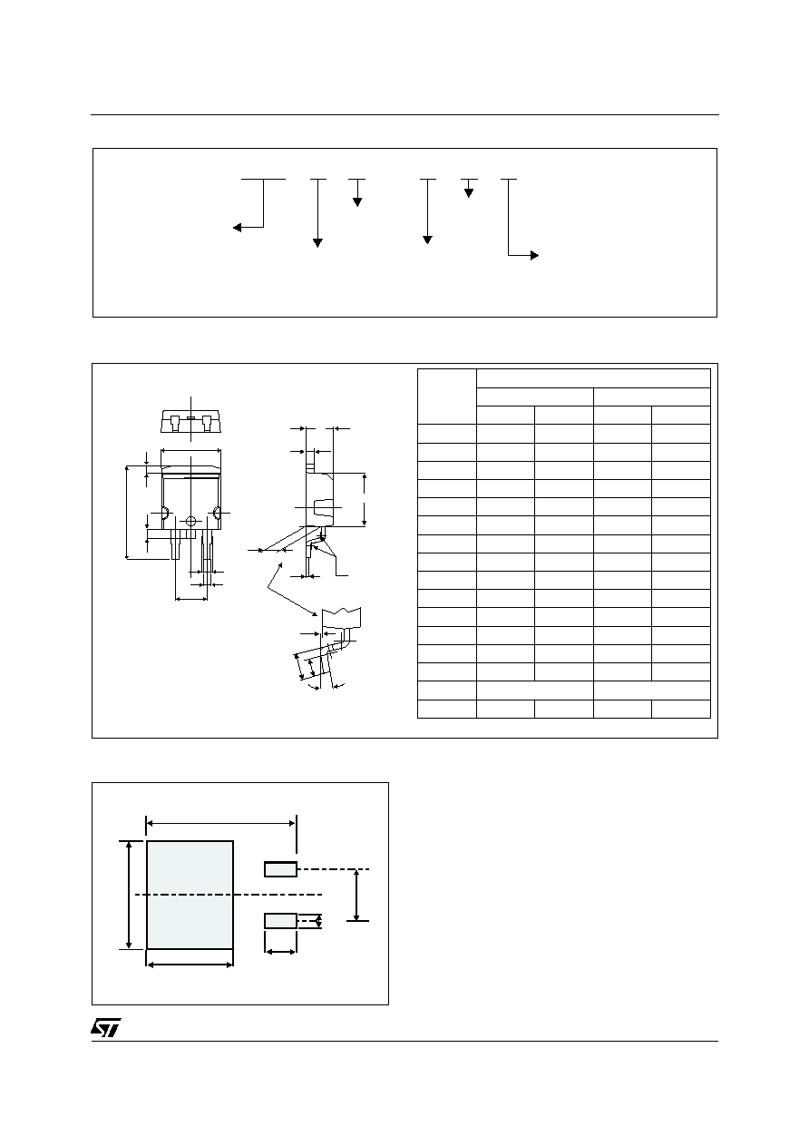
PACKAGE MECHANICAL DATA
D
2
PAK
Plastic
A
C2
D
R
A2
M
V2
C
A1
G
L
L3
L2
B
B2
E
*
* FLAT ZONE NO LESS THAN 2mm
REF.
DIMENSIONS
Millimeters
Inches
Min.
Max.
Min.
Max.
A
4.40
4.60
0.173
0.181
A1
2.49
2.69
0.098
0.106
A2
0.03
0.23
0.001
0.009
B
0.70
0.93
0.027
0.037
B2
1.14
1.70
0.045
0.067
C
0.45
0.60
0.017
0.024
C2
1.23
1.36
0.048
0.054
D
8.95
9.35
0.352
0.368
E
10.00
10.40
0.393
0.409
G
4.88
5.28
0.192
0.208
L
15.00
15.85
0.590
0.624
L2
1.27
1.40
0.050
0.055
L3
1.40
1.75
0.055
0.069
M
2.40
3.20
0.094
0.126
R
0.40 typ.
0.016 typ.
V2
0∞
8∞
0∞
8∞
8.90
3.70
1.30
5.08
16.90
10.30
FOOTPRINT DIMENSIONS (in millimeters)
ACS
T 6 - 7 S
T
AC Switch
Topology: Triac
I
6A
T(RMS):
V
700V
DRM:
I
S = 10mA
GT
Package
T: TO-220AB
G: D PAK
FP: TO-220FPAB
R: I PAK
2
2
ORDERING INFORMATION
ACST6-7S
8/9
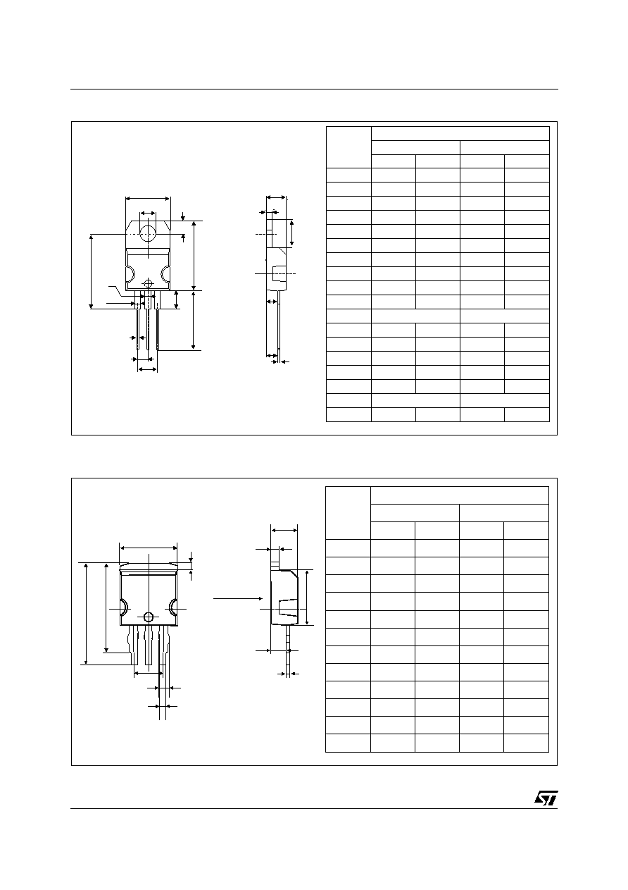
PACKAGE MECHANICAL DATA
TO-220AB (Plastic)
A
C
D
L7
Dia
L5
L6
L9
L4
F
H2
G
G1
L2
F2
F1
E
M
REF.
DIMENSIONS
Millimeters
Inches
Min.
Max.
Min.
Max.
A
4.40
4.60
0.173
0.181
C
1.23
1.32
0.048
0.051
D
2.40
2.72
0.094
0.107
E
0.49
0.70
0.019
0.027
F
0.61
0.88
0.024
0.034
F1
1.14
1.70
0.044
0.066
F2
1.14
1.70
0.044
0.066
G
4.95
5.15
0.194
0.202
G1
2.40
2.70
0.094
0.106
H2
10
10.40
0.393
0.409
L2
16.4 typ.
0.645 typ.
L4
13
14
0.511
0.551
L5
2.65
2.95
0.104
0.116
L6
15.25
15.75
0.600
0.620
L7
6.20
6.60
0.244
0.259
L9
3.50
3.93
0.137
0.154
M
2.6 typ.
0.102 typ.
Diam.
3.75
3.85
0.147
0.151
PACKAGE MECHANICAL DATA
I
2
PAK
L2
E
L3
L
G
B2
B
D
A
C2
A1
C
Note 2
Note 2
Cropping
Direction
REF.
DIMENSIONS
Millimeters
Inches
Min.
Max.
Min.
Max.
A
4.40
4.60
0.173
0.181
A1
2.49
2.69
0.098
0.106
B
0.70
0.93
0.027
0.037
B2
1.14
1.7
0.045
0.067
C
0.45
0.60
0.018
0.024
C2
1.23
1.36
0.048
0.053
D
8.95
9.35
0.352
0.368
E
10.0
10.4
0.394
0.409
G
4.88
5.28
0.192
0.208
L
16.7
17.5
0.657
0.689
L2
1.27
1.40
0.050
0.055
L3
13.82
14.42
0.544
0.568
ACST6-7S
9/9
Information furnished is believed to be accurate and reliable. However, STMicroelectronics assumes no responsibility for the consequences of
use of such information nor for any infringement of patents or other rights of third parties which may result from its use. No license is granted by
implication or otherwise under any patent or patent rights of STMicroelectronics. Specifications mentioned in this publication are subject to
change without notice. This publication supersedes and replaces all information previously supplied.
STMicroelectronics products are not authorized for use as critical components in life support devices or systems without express written ap-
proval of STMicroelectronics.
The ST logo is a registered trademark of STMicroelectronics
© 2002 STMicroelectronics - Printed in Italy - All rights reserved.
STMicroelectronics GROUP OF COMPANIES
Australia - Brazil - Canada - China - Finland - France - Germany
Hong Kong - India - Israel - Italy - Japan - Malaysia - Malta - Morocco - Singapore
Spain - Sweden - Switzerland - United Kingdom - United States.
http://www.st.com
Ordering type
Marking
Package
Weight
Base qty
Delivery mode
ACST6-7ST
ACST67S
TO-220AB
2.3 g
50
Tube
ACST6-7SG
ACST67S
D
2
PAK
1.5 g
50
Tube
ACST6-7SFP
ACST67S
TO-220FPAB
2.4 g
50
Tube
ACST6-7SR
ACST67S
I
2
PAK
1.5 g
50
Tube
s
Epoxy meets UL94,V0
OTHER INFORMATION
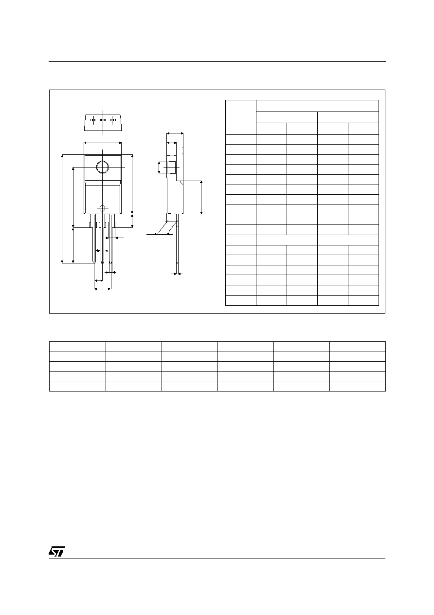
PACKAGE MECHANICAL DATA
TO-220FPAB (Plastic)
H
L3
L2
L4
L6
G
G1
F
F1
L5
D
E
L7
A
B
Dia
F2
REF.
DIMENSIONS
Millimeters
Inches
Min.
Max.
Min.
Max.
A
4.4
4.6
0.173
0.181
B
2.5
2.7
0.098
0.106
D
2.5
2.75
0.098
0.108
E
0.45
0.70
0.018
0.027
F
0.75
1
0.030
0.039
F1
1.15
1.70
0.045
0.067
F2
1.15
1.70
0.045
0.067
G
4.95
5.20
0.195
0.205
G1
2.4
2.7
0.094
0.106
H
10
10.4
0.393
0.409
L2
16 Typ.
0.63 Typ.
L3
28.6
30.6
1.126
1.205
L4
9.8
10.6
0.386
0.417
L5
2.9
3.6
0.114
0.142
L6
15.9
16.4
0.626
0.646
L7
9.00
9.30
0.354
0.366
Dia.
3.00
3.20
0.118
0.126