 | –≠–ª–µ–∫—Ç—Ä–æ–Ω–Ω—ã–π –∫–æ–º–ø–æ–Ω–µ–Ω—Ç: ACST8-8CT | –°–∫–∞—á–∞—Ç—å:  PDF PDF  ZIP ZIP |
Æ
1/10
ACST8
November 2004
MAIN APPLICATIONS
AC static switching in appliance & industrial
control systems
Washing machine with bi-rotational induction
motor drive
Induction motor drive for:
- refrigerator / freezer compressor
- air conditioning compressor
FEATURES
V
DRM
/V
RRM
= +/- 800V
Avalanche controlled device
I
T(RMS)
= 8A with T
CASE
= 90 ∞C
High noise immunity: static dV/dt > 750 V/µs
Gate triggering current : I
GT
< 30 mA
Snubberless turn off commutation:
(dI/dt)c > 4.5A/ms
BENEFITS
Enables equipment to meet EN61000-4-5
standard
High off-state reliability with planar technology
Need no external overvoltage protection
Reduces the power component count
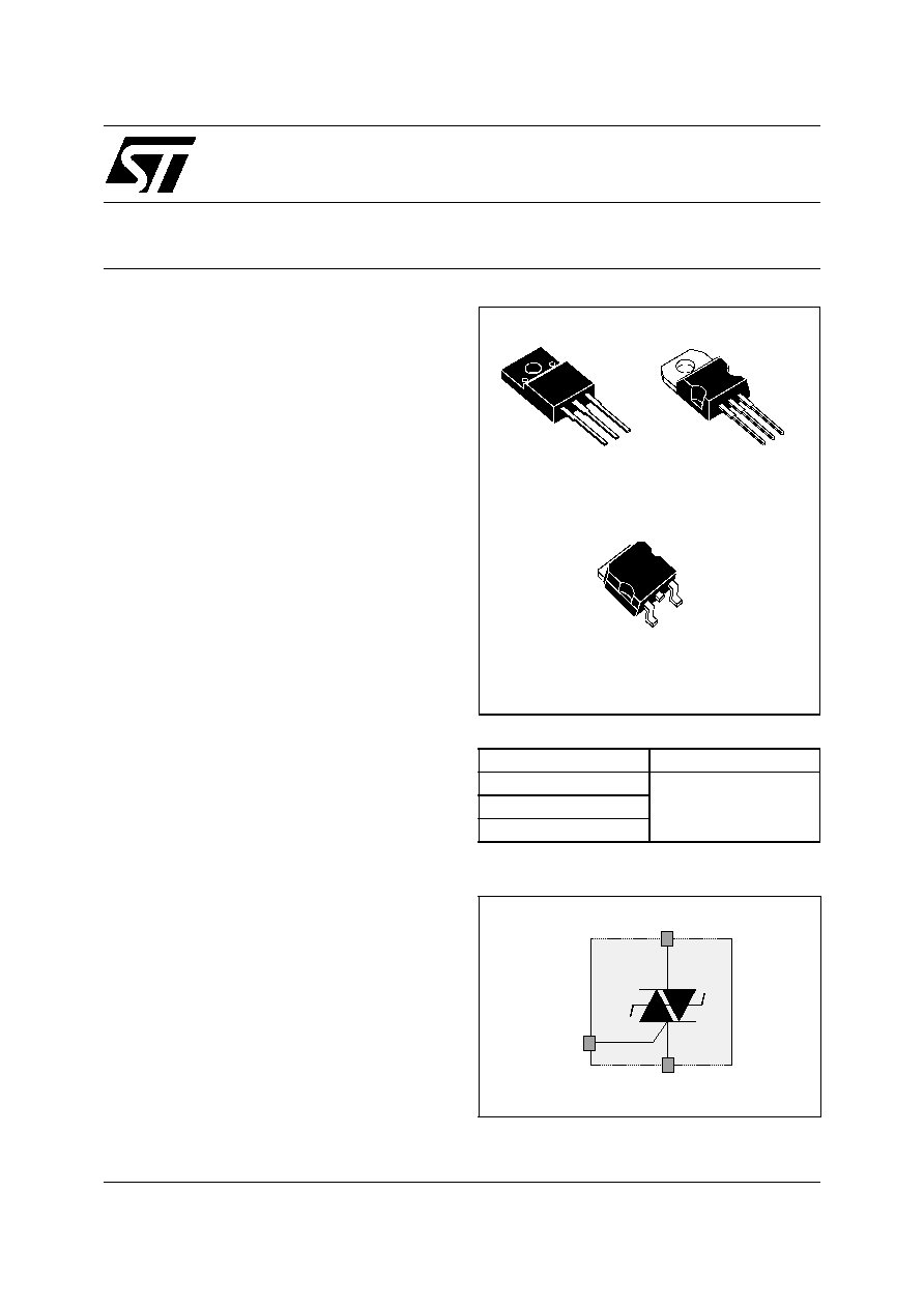
DESCRIPTION
The ACST8-8C belongs to the AC power switch
family built around the ASD
TM
technology. This
high performance device is adapted to home appli-
ances or industrial systems and drives an induc-
tion motor up to 8A.
This ACST switch embeds a triac structure with a
high voltage clamping device to absorb the induc-
tive turn off energy and withstand line transients
such as those described in the IEC61000-4-5
standards.
OVER VOLTAGE PROTECTED
AC POWER SWITCH
COM
OUT
OUT
G
TO-220FPAB
ACST8-8CFP
TO-220AB
ACST8-8CT
G
OUT
COM
D
2
PAK
ACST8-8CG
COM
OUT
G
Table 1: Order Codes
Part Number
Marking
ACST8-8CFP
ACST88C
ACST8-8CT
ACST8-8CG
Figure 1: Functional Diagram
G
COM
OUT
TM: ASD is a trademark of STMicroelectronics.
REV. 6
ASDTM
(AC Switch Family)
ACST8
2/10
Table 2: Absolute Ratings (limiting values)
Note 1: according to test described by IEC61000-4-5 standard & figure A.
Table 3: Gate Characteristics (maximum values)
Table 4: Thermal Resistance
Table 5: Parameter Description
Symbol
Parameter
Value
Unit
I
T(RMS)
RMS on-state current full cycle sine
wave 50 to 60 Hz
TO-220FPAB
Tcase = 90∞C
8
A
TO-220AB /
D
2
PAK
Tcase = 100∞C
8
I
TSM
Non repetitive surge peak on-state current
T
j
initial = 25∞C, full cycle sine wave
t
p
= 20ms
80
A
t
p
= 16.7ms
85
A
I
2
t
Thermal constraint for fuse selection
tp = 10ms
35
A
2
s
dI/dt
Non repetitive on-state current critical rate of rise
I
G
= 10mA (t
r
< 100ns)
Rate period > 1mn
100
A/µs
V
PP
Non repetitive line peak pulse voltage
note 1
2
kV
T
stg
Storage temperature range
- 40 to + 150
∞C
T
j
Operating junction temperature range
- 40 to + 125
∞C
T
l
Maximum lead soldering temperature during 10s
260
∞C
Symbol
Parameter
Value
Unit
P
G (AV)
Average gate power dissipation
0.1
W
P
GM
Peak gate power dissipation (t
p
= 20µs)
10
W
I
GM
Peak gate current (t
p
= 20µs)
1
A
Symbol
Parameter
Value
Unit
R
th(j-a)
Junction to ambient
TO-220FPAB
TO-220AB
60 ∞C/W
R
th(j-a)
Junction to ambien (soldered on 1 cm
2
copper pad) D
2
PAK
45
∞C/W
R
th(j-c)
Junction to case for full cycle sine wave conduction TO-220FPAB
3.5
∞C/W
R
th(j-c)
Junction to case for full cycle sine wave conduction
TO-220AB
D
2
PAK
2.5 ∞C/W
Parameter Symbol
Parameter description
I
GT
Gate triggering current
V
GT
Gate triggering voltage
V
GD
Non triggering voltage
I
H
Holding current
I
L
Latching current
V
TM
On state voltage
V
T0
On state characteristic threshold voltage
R
d
On state characteristic dynamic resistance
I
DRM
/
I
RRM
Forward or reverse leakage current
dV/dt
Static pin OUT voltage rise
(dI/dt)c
Turn off current rate of decay
V
CL
Avalanche voltage at turn off
ACST8
3/10
Table 6: Electrical Characteristics per Switch
For either positive or negative polary of pin OUT voltage respect to pin COM voltage
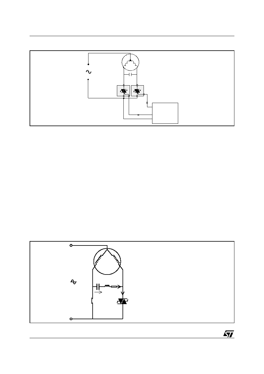
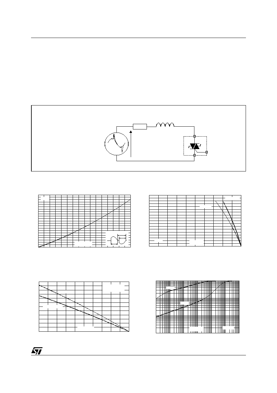
1. AC LINE SWITCH BASIC APPLICATION
The ACST8-8C device is especially designed to drive medium power induction motors in washing ma-
chines, refrigerators, dish washers, and tumble dryers.
Pin COM
: Common drive reference, to be connected to the power line neutral
Pin G
: Switch Gate input to be connected to the controller
Pin OUT
: Switch Output to be connected to the load
When driven from a low voltage controller, the ACST switch is triggered with a negative gate current flow-
ing out of the gate pin G. It can be driven by the controller through a resistor as shown on the typical appli-
cation diagram. In appliance systems, the ACST8-8C switch intends to drive medium power load in ON /
OFF full cycle or phase angle control mode.
Thanks to its thermal and turn-off commutation characteristics, the ACST8-8C switch is able to drive an
inductive load up to 8A without a turn-off aid snubber circuit.
In washing machine or drier appliances, the tumble rotates in both directions. When using bidirectional
phase shift induction motor, two switches are connected on each side of the phase shift capacitor: in
steady-state operation, one switch only conducts energising the coils and defining the tumble direction.
Symbol
Test conditions
Values
Unit
V
DRM
/
V
RRM
Repetitive peak off-state voltage
MAX.
800
V
I
GT
V
OUT
= 12V (DC) R
L
= 33
T
j
= 25∞C
MAX.
30
mA
V
GT
V
OUT
= 12V (DC) R
L
= 33
T
j
= 25∞C
MAX.
1.5
V
V
GD
V
OUT
= V
DRM
R
L
= 3.3k
T
j
= 125∞C
MIN.
0.2
V
I
H
I
OUT
= 100mA
Gate open
T
j
= 25∞C
MAX.
40
mA
I
L
I
G
= 20mA
T
j
= 25∞C
MAX.
70
mA
V
TM
I
OUT
= 11A
t
p
= 380µs
T
j
= 25∞C
MAX.
1.5
V
V
T0
T
j
= 125∞C
MAX.
0.95
V
R
d
T
j
= 125∞C
MAX.
50
m
I
DRM
/
I
RRM
V
OUT
= V
DRM
V
OUT
= V
RRM
T
j
= 25∞C
MAX.
10
µA
T
j
= 125∞C
MAX.
1
mA
dV/dt
V
OUT
= 550V
gate open
T
j
= 125∞C
MIN.
750
V/µs
(dI/dt)c
Without snubber
T
j
= 125∞C
MIN.
4.5
A/ms
V
CL
I
CL
= 1mA
t
p
= 1ms
T
j
= 25∞C
TYP.
1200
V
ACST8
4/10
Figure 2: Typical Application Diagram
2. ROBUSTNESS AGAINST FAST CAPACITOR DISCHARGE
When parasitic transients or controller mis-operation occur, the blocked switch may turn on by spurious
switch firing. Since the phase shift capacitor is charged, its energy is instantaneously dissipated through
the two ACSTs which can be destroyed. To prevent such a failure, a resistive inductive circuit R-L is added
in series with the phase shift capacitor.
The dI/dt depends on the maximal voltage V
max
of the phase shift capacitor (700V on 240V mains appli-
cations), and on the inductance L:
The total switch turn on di/dt is the sum of the di/dt created by any RC noise suppressor discharge and
the dI/dt created by the motor capacitor discharge.
Since the maximal dI/dt capability at turn-on of the ACST8 is 100A/µs, the motor capacitor di/dt is assumed
to be less than 50A/µs; therefore, the inductance should be 14µH.
The resistor R limits the surge current through the ACST8 during the capacitor discharge according to the
specified curve I
TSM
= f (tp) as shown in figure 11
(to be issued)
, and 1.2
is low enough to limit the resistor
dissipation (usually less than 1 W).
Finally both the 14µH inductance and the 1.2
resistance provide a safety margin of two on the surge cur-
rent I
TSM
described in figure 11.
CONTROL
UNIT
COM
OUT
G
dl
dt
----
v
max
L
-----------
=
C
L
V
AC
T1
T2
ON
R
700V
M
Fast capacitor discharge when
one ACST switch turns on (T2)
and the motor runs (T1 ON).
ACST8
5/10
3. AC LINE TRANSIENT VOLTAGE RUGGEDNESS
The ACST8-8C switch is able to safely withstand the AC line transient voltages either by clamping the low
energy spikes or by breaking over under high energy shocks.
The test circuit in figure 3 is representative of the ACST application and is used to test the ACST switch
according to the IEC61000-4-5 standard conditions. Thanks to the load impedance, the ACST switch with-
stands voltage spikes up to 2 kV above the peak line voltage by breaking over safely. Such non repetitive
testing can be done 10 times on each AC line voltage polarity.
Figure 3: Overvoltage ruggedness test circuit for resistive and inductive loads according to
IEC61000-4-5 standard R = 47
, L = 10µH & V
PP
= 2kV
Figure 4: Maximum power dissipation versus
RMS on-state current
Figure 5: RMS on-state current versus case
temperature
Figure 6: RMS on-state current versus ambient
temperature
Figure 7: Relative variation of thermal
impedance versus pulse duration (TO-220FPAB)
L
R
V
AC
+ V
PP
SURGE VOLTAGE
AC LINE & GENERATOR
G
COM
OUT
0
1
2
3
4
5
6
7
8
9
10
11
0
1
2
3
4
5
6
7
8
=180∞
180∞
P(W)
I
(A)
T(RMS)
0
1
2
3
4
5
6
7
8
9
0
25
50
75
100
125
=180∞
TO-220AB/D PAK
2
TO-220FPAB
I
(A)
T(RMS)
T (∞C)
C
0.0
0.5
1.0
1.5
2.0
2.5
3.0
0
25
50
75
100
125
=180∞
Printed circuit board FR4
Natural convection
D PAK
2
TO-220FPAB/TO-220AB
I
(A)
T(RMS)
T
(∞C)
amb
1.E-03
1.E-02
1.E-01
1.E+00
1.E-03
1.E-02
1.E-01
1.E+00
1.E+01
1.E+02
1.E+03
TO-220FPAB
K=[Z /R ]
th
th
t (∞C)
p
Z
th(j-c)
Z
th(j-a)