 | –≠–ª–µ–∫—Ç—Ä–æ–Ω–Ω—ã–π –∫–æ–º–ø–æ–Ω–µ–Ω—Ç: ADE3000 | –°–∫–∞—á–∞—Ç—å:  PDF PDF  ZIP ZIP |
October 2003
1/88
ADE3000 ADE3050 ADE3100
ADE3200 ADE3250 ADE3300
LCD Display Engines
with Integrated DVI, ADC and YUV Ports
Æ
The ADE3xxx is a family of highly integrated display engine ICs, enabling the most advanced, flexible, and
cost-effective system-on-chip solutions for LCD display applications. The ADE3xxx line-up covers the full
range of applications from XGA analog only to dual SXGA Smart Panel designs. All twelve ADE3xxx
devices are pin-to-pin compatible and use a common software platform.
Feature Overview
s
Programmable Context SensitiveTM Scaling
s
High-quality up-scaling and down-scaling
s
Dual Input: DVI / VGA
s
Integrated 9-bit ADC/PLL
s
Integrated DVI-Rx
s
IQSyncTM AutoSetup
s
Integrated programmable timing controller
s
Integrated Pattern generator
s
Perfect PictureTM Technology
s
sRGB 3D Color Warp
s
Integrated OSD
s
Advanced EMI reduction features
s
Framelock operation with Safety ModeTM
s
Serial I≤C interface
s
Low power 0.18 µm process technology
Product Selector
208-pin PQFP Package
Product
Input Interface Support
Output Format Support
Analog
DVI
YUV
Resolution
TCON
ADE3000
x
x
Up to XGA 75Hz
ADE3000T
x
x
Up to XGA 75Hz
x
ADE3000SX
x
x
Up to SXGA 75Hz
ADE3000SXT
x
x
Up to SXGA 75Hz
x
ADE3050
x
x
Up to XGA 75Hz
ADE3050T
x
x
Up to XGA 75Hz
x
ADE3050SX
x
x
Up to SXGA 75Hz
ADE3050SXT
x
x
Up to SXGA 75Hz
x
ADE3100
x
x
x
Up to XGA 75Hz
ADE3200
x
x
x
Up to XGA 75Hz
x
ADE3250
x
x
x
Up to SXGA 75Hz
x
ADE3300
x
x
x
Up to SXGA 75Hz

ADE3XXX
2/88
Third Generation Context SensitiveTM Scaler
q
Sharper text with Edge Enhancement
q
RAM based coefficients for unique
customization
q
5:1 upscale and 2:1 downscale
q
Independent X - Y axis zoom and shrink
q
Bob de-interlacing eliminates jaggies and
motion artifacts
Analog RGB input
q
140MHz 9-bit ADC
q
Ultra low jitter digital linelock PLL
q
Composite Sync and Sync on Green support
Secure DVITM Receiver
q
Single Link DVI receiver
q
Input Pixel Rate from 25 to140 MHz
q
Low power mode with activity detection
q
Compatibility with all DVI compliant
transmitters
Digital TV Video Input
q
VESA VIP 1.1, 2.0 and CCIR656 compliant
q
25 to 75 MHz input clock
IQsyncTM AutoSetup
q
AutoSetup configures phase, clock, level, and
position
q
Supports continuous calibration for reduced
user intervention
q
Detects activity on all inputs and selects the
active source
q
Compatible with all standard VESA and GTF
modes
Perfect PictureTM Technology
q
Video & Picture highlight zoning
q
Supports up to 7 different windows
q
Independent window controls for contrast
brightness, sharpness, and color
Perfect ColorTM Technology
q
Programmable 3D color warp
q
Digital brightness, contrast, hue, and
saturation gamma controls for all inputs
q
Simple white point control
q
Compatible with sRGB standard
q
True color dithering for 12- and 18-bit panels
q
Temporal and spatial dithering
q
30-bit programmable gamma table
OSD Engine
q
256 RAM based 12x18 characters
q
1 and 4-bit per pixel color characters
q
Bordering, shadowing, transparency, fade-in,
and fade-out
q
Supports font rotation
q
Up to 4 sub windows
q
32 entry TrueColor LUT
Programmable Timing Controller (TCON)
q
Highly-programmable support for XGA, TTL
and RSDS SmartPanels
q
Dual function TTL and RSDS outputs
q
Advanced flicker detection and reduction
q
12 programmable timing signals for row/
column control
q
Wide range of drivers & TCON compatibility
q
Simulation tools for easy programming
q
Supports complex polarity generation for IPS
panels
Advanced EMI Reduction Features
q
Flexible data inversion / transition
minimization, single, dual, and separate
q
Per pin delay, 0 to 6ns in 0.4ns increments
q
Adaptive Slew Rate control outputs
q
Supports 18/24/36/48-bit RSDS outputs
q
Differential clock
q
Spread spectrum -programmable digital FM
modulation of the output clock with no
external components
Output Format
q
Supports resolutions up to SXGA @ 75Hz
q
Supports 6 or 8-bit Panels
q
Support double or single pixel wide formats

3/88
ADE3XXX
Table of Contents
Chapter 1
General Description . . . . . . . . . . . . . . . . . . . . . . . . . . . . . . . . . . . . . . . . . . . . . . . .5
1.1
Pin Description .................................................................................................................... 6
Chapter 2
ADE3XXX Functional Description . . . . . . . . . . . . . . . . . . . . . . . . . . . . . . . . . . . .13
2.1
Global Control Block .......................................................................................................... 13
2.2
FM Frequency Synthesizer ................................................................................................ 17
2.3
ADC Block .......................................................................................................................... 18
2.4
Line Lock PLL Block ........................................................................................................... 19
2.5
Digital Video Input (DVI) ..................................................................................................... 22
2.6
HDCP Block ....................................................................................................................... 27
2.7
YUV Block .......................................................................................................................... 29
2.8
Sync Retiming Block .......................................................................................................... 30
2.9
Sync Measurement Block .................................................................................................. 32
2.10
Sync Mux Block .................................................................................................................. 40
2.11
Data Mux Block .................................................................................................................. 42
2.12
Data Measurement Block ................................................................................................... 42
2.12.1
Edge Intensity ....................................................................................................................................43
2.12.2
Pixel Sum ...........................................................................................................................................43
2.12.3
Min / Max ...........................................................................................................................................43
2.12.4
PCD ...................................................................................................................................................43
2.12.5
H Position Min / Max ..........................................................................................................................43
2.12.6
V Position Min / Max ..........................................................................................................................44
2.12.7
DE Size ..............................................................................................................................................44
2.13
Programmable Nonlinearity Block ...................................................................................... 48
2.14
Scaler Block ....................................................................................................................... 49
2.15
Output Sequencer Block .................................................................................................... 52
Frame Synchronization .......................................................................................................................................52
Timing Unit ..........................................................................................................................................................52
Signal Generation ...............................................................................................................................................52
2.16
Timing Controller (TCON) Block ........................................................................................ 55
2.17
Pattern Generator Block ..................................................................................................... 60
Screen Split ........................................................................................................................................................60
Pattern Engine ....................................................................................................................................................61
Borders ...............................................................................................................................................................61

ADE3XXX
4/88
2.18
SRGB Block ........................................................................................................................64
2.18.1
Parametric Gamma Correction and Digital Contrast/Brightness Control .......................................... 64
2.18.2
Color Space Warp ............................................................................................................................. 64
2.19
OSD Block ..........................................................................................................................66
2.20
Flicker Block .......................................................................................................................72
2.21
Gamma Block .....................................................................................................................74
2.22
APC Block ..........................................................................................................................74
2.23
Output Mux Block ...............................................................................................................75
2.24
Pulse Width Modulation (PWM) Block ................................................................................77
2.25
DFT Block ...........................................................................................................................79
2.26
I≤C RAM Addresses ...........................................................................................................80
Chapter 3
Electrical Specifications . . . . . . . . . . . . . . . . . . . . . . . . . . . . . . . . . . . . . . . . . . . 82
3.1
Absolute Maximum Ratings ................................................................................................82
3.2
Power Consumption Matrices .............................................................................................82
3.3
Nominal Operating Conditions ............................................................................................83
3.4
Preliminary Thermal Data ...................................................................................................84
3.5
Preliminary DC Specifications ............................................................................................84
3.5.1
LVTTL 5 Volt Tolerant Inputs With Hysteresis ................................................................................... 84
3.5.2
LVTTL 5 Volt Tolerant Inputs ............................................................................................................. 84
3.5.3
LVTTL 5 Volt Tolerant I/O With Hysteresis ........................................................................................ 84
3.5.4
LVTTL Outputs .................................................................................................................................. 84
3.6
Preliminary AC Specifications ...........................................................................................85
Chapter 4
Package Mechanical Data . . . . . . . . . . . . . . . . . . . . . . . . . . . . . . . . . . . . . . . . . . 86
Chapter 5
Revision History . . . . . . . . . . . . . . . . . . . . . . . . . . . . . . . . . . . . . . . . . . . . . . . . . 87
5/88
ADE3XXX
1
General Description
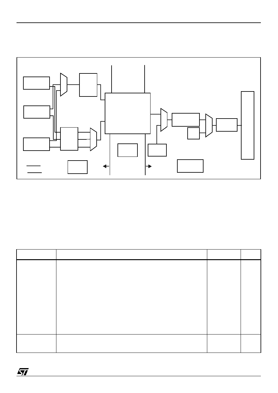
The ADE3XXX family of devices is capable of implementing all of the advanced features of today's
LCD monitor products. For maximum flexibility, an external microcontroller (MCU) is used for
controlling the ADE3XXX and other monitor functions.
The ADE3XXX architecture unburdens the MCU from all data-intensive pixel manipulations,
providing an optimal blend of feature and code customization without incurring the cost of a 16-bit
processor or memory. The key interactions between the monitor MCU and the ADE3XXX can be
broken down into the features shown in the table below.
Figure 1: ADE3XXX Block Diagram
Table 1: ADE3xxx Features (Sheet 1 of 2)
Feature
Description of ADE3XXX Operation
Blocks Used
Pages
Power Up / Initialize When power is first applied, the ADE3XXX is asynchronously reset from a pin.
The MCU typically programs the ADE3XXX with a number of default values and
sets up the ADE3XXX to identify activity on any of the input pins. All
preconfigured values and RAMs, such as DVI settings, line-lock PLL settings,
video input modes (YUV), OSD characters, LCD timing values (output
sequencer), scale kernels, gamma curves, sRGB color warp, APC dithering,
output pin configuration (OMUX), etc. can be preloaded into the ADE3XXX. The
typical end state is that the ADE3XXX is initialized into a low power mode, ready
to turn active once the power button is pressed.
GLBL
SMEAS
DVI
LLK
ADC
YUV
OSD
SCALER
GAMMA
SRGB
OUTSEQ
TCON
APC
OMUX
13
32
22
19
18
29
66
49
74
64
52
55
74
75
Activity Detect
When the monitor has been powered on, the inputs can be monitored for active
video sources. Based on the activity monitors, the MCU chooses an input or
power down state.
SMEAS
32
YUV Port
Analog Port
DVI Port
Scaler with
SCLK
F. Synth
P. Gen
Out
p
ut
For
m
at
FM
F. Synth
LLKPLL
DMEAS
SMEAS
INCLK
SCLK
DOTCLK
Color
Management
OSD
Gamma
LUT
DATA
CTRL
Vertical Keystone