REV. 0
a
Information furnished by Analog Devices is believed to be accurate and
reliable. However, no responsibility is assumed by Analog Devices for its
use, nor for any infringements of patents or other rights of third parties that
may result from its use. No license is granted by implication or otherwise
under any patent or patent rights of Analog Devices.
One Technology Way, P.O. Box 9106, Norwood, MA 02062-9106, U.S.A.
Tel: 781/329-4700
www.analog.com
Fax: 781/326-8703
© Analog Devices, Inc., 2002
SST-Melody
Æ
-SHARC
Æ
High End, Multichannel,
32-Bit Floating-Point Audio Processor
GENERAL DESCRIPTION
The SST-Melody-SHARC family of powerful 32-bit Audio Proces-
sors from Analog Devices provides flexible solutions and delivers
a host of features across high end and high fidelity audio systems
to the AV receiver and DVD markets. It includes multichannel
audio decoders, encoders, and post processors for digital
audio designs using DSP chipsets in home theater systems and
automotive audio receivers.
(continued on page 11)
FEATURES
Super Harvard Architecture Computer (SHARC)
4 Independent Buses for Dual Data, Instruction, and
I/O Fetch on a Single Cycle
32-Bit Fixed-Point Arithmetic; 32-Bit and 40-Bit Floating-
Point Arithmetic
544 Kbits On-Chip SRAM Memory, Integrated I/O
Peripheral I
2
S Support for 8 Simultaneous Receive and
Transmit Channels
66 MIPS, 198 MFLOPS Peak, 132 MFLOPS Sustained
Performance
User-Configurable 544 Kbits On-Chip SRAM Memory
2 External Port, DMA Channels and 8 Serial Port,
DMA Channels
Decodes Industry Standard Formats Using a 32-Bit
Floating Point Implementation for Decoding
Dolby
Æ
Digital AC-3, Dolby Digital EX Processing
Dolby Pro Logic
Æ
, 96 kHz, Dolby Pro Logic II
Dolby Headphone, Dolby 3/0
DTS
Æ
5.1, DTS-ES
Æ
-Discreet 6.1, DTS Matrix and Matrix 3.0,
DTS 96/24
Æ
, DTS NEO:6
THX
Æ
Ultra, Select, Ultra2, 5.1, 7.1, EX
SRS
Æ
Labs Circle Surround II
TM
, Virtual Loudspeaker
MPEG AAC, MPEG2 Decode, MPEG 2-Channel Decode
PCM, PCM 96 kHz
HDCD, MLP*
Delay 7.1, 96 kHz
Bass 7.1, 96 kHz, Bass/Treble 2 Channel
ADI Surround: Club, Music, and Stadium
AAC (LC), AAC (LC) 2 Channel, AAC MP
WaveSurround 5.1 Channel to Headphone, Stereo to
Headphone, Channel to Loudspeaker, Stereo to
Loudspeaker
Downsampling 96 kHz to 48 kHz (2-Channel)
3-Band Equalizer, 2-Channel
Encoders: AC-3 2-Channel Consumer Encoder
Single Chip DSP-Based Implementation of Digital Audio
Algorithms
I
2
S Compatible Ports
Interface to External SDRAM
Easy Interfaces to Audio Codecs
96 kHz Processing
Supports Customer Specific Post Processing
Automatic Stream Detection and Code Loading
Easy to Use Software Architecture
Optimized Library of Routines
Host Communication Using 16-Bit Parallel Port or SPI Port
Highly Flexible Serial Ports
SRAM Interface for More Delay
Supports IEC60958 For Bit Streams
8-Channel Output Using TDM Codecs
APPLICATIONS
Home Theater AVR Systems
Automotive Audio Receivers
Video Game Consoles
DVD Players
Cable and Satellite Set-Top Boxes
Multimedia Audio/Video Gateways
Melody and SHARC are registered trademarks of Analog Devices, Inc.
DTS, DTS-ES, and DTS 96/24 are registered trademarks of Digital Theater
Systems, Inc.
Dolby and Pro Logic are registered trademarks of Dolby Laboratories
Licensing Corporation.
SRS is a registered trademark and Circle Surround II is a trademark of SRS Labs.
THX is a registered trademark of the THX, Ltd.
*MLP is implemented, not certified.
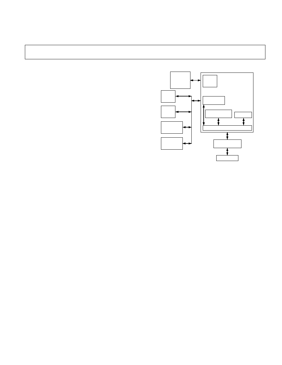
FUNCTIONAL BLOCK DIAGRAM
SDRAM
128K 32,
BOOT ROM
1M 8
ADC
DAC
S/PDIF
TRANSMITTER
S/PDIF
RECEIVER
IRQ
GPIO
SERIAL PORT
ALGORITHMS
COMMAND
KERNEL
DMA CONNECTION
OR DUAL BUFFER
HOST MICRO
SST-Melody-SHARC

REV. 0
≠2≠
SST-Melody-SHARC≠SPECIFICATIONS
RECOMMENDED OPERATING CONDITIONS
1
Test
C Grade
K Grade
Parameter
Conditions
Min
Max
Min
Max
Unit
V
DD
Supply Voltage
3.13
3.60
3.13
3.60
V
T
CASE
Case Operating Temperature
≠40
+100
0
+85
∞C
V
IH
High Level Input Voltage
@ V
DD
= max
2.0
V
DD
+ 0.5
2.0
V
DD
+ 0.5 V
V
IL1
Low Level Input Voltage
2
@ V
DD
= min
≠0.5
+0.8
≠0.5
+0.8
V
V
IL2
Low Level Input Voltage
3
@ V
DD
= min
≠0.5
+0.7
≠0.5
+0.7
V
NOTES
1
See Environmental Conditions section for information on thermal specifications.
2
Applies to input and bidirectional pins: DATA31≠0, ADDR23≠0, BSEL,
RD, WR, SW, ACK, SBTS, IRQ2≠0, FLAG11≠0, HBG, CS, DMAR1, DMAR2, BR2≠1, ID2≠0,
RPBA,
CPA, TFS0, TFS1, RFS0, RFS1, BMS, TMS, TDI, TCK, HBR, DR0A, DR1A, DR0B, DR1B, TCLK0, TCLK1, RCLK0, RCLK1, RESET, TRST,
PWM_EVENT0, PWM_EVENT1,
RAS, CAS, SDWE, SDCKE.
3
Applies to input pin CLKIN.
ELECTRICAL CHARACTERISTICS
C and K Grades
Parameter
Test Conditions
Min
Max
Unit
V
OH
High Level Output Voltage
1
@ V
DD
= min, I
OH
= ≠2.0 mA
2
2.4
V
V
OL
Low Level Output Voltage
1
@ V
DD
= min, I
OL
= +4.0 mA
2
0.4
V
I
IH
High Level Input Current
3
@ V
DD
= max, V
IN
= V
DD
max
10
µA
I
IL
Low Level Input Current
3
@ V
DD
= max, V
IN
= 0 V
10
µA
I
ILP
Low Level Input Current
4
@ V
DD
= max, V
IN
= 0 V
150
µA
I
OZH
Three-State Leakage Current
5, 6,
7, 8
@ V
DD
= max, V
IN
= V
DD
max
10
µA
I
OZL
Three-State Leakage Current
5
@ V
DD
= max, V
IN
= 0 V
8
µA
I
OZLS
Three-State Leakage Current
6
@ V
DD
= max, V
IN
= 0 V
150
µA
I
OZLA
Three-State Leakage Current
9
@ V
DD
= max, V
IN
= 1.5 V
350
µA
I
OZLAR
Three-State Leakage Current
8
@ V
DD
= max, V
IN
= 0 V
4
mA
I
OZLC
Three-State Leakage Current
7
@ V
DD
= max, V
IN
= 0 V
1.5
mA
C
IN
Input Capacitance
10, 11
f
IN
= 1 MHz, T
CASE
= 25
∞C, V
IN
= 2.5 V
8
pF
NOTES
1
Applies to output and bidirectional pins: DATA31≠0, ADDR 23≠0,
MS3≠0, RD, WR, SW, ACK, FLAG11≠0, HBG, REDY, DMAG1, DMAG2, BR2≠1, CPA,
TCLK0, TCLK1, RCLK0, RCLK1, TFS0, TFS1, RFS0, RFS1, DT0A, DT1A, DT0B, DT1B, XTAL,
BMS, TDO, EMU, BMSTR, PWM_EVENT0,
PWM_EVENT1,
RAS, CAS, DQM, SDWE, SDCLK0, SDCLK1, SDCKE, SDA10.
2
See Output Drive Current section for typical drive current capabilities.
3
Applies to input pins: ACK,
SBTS, IRQ2≠0, HBR, CS, DMAR1, DMAR2, ID1≠0, BSEL, CLKIN, RESET, TCK (Note that ACK is pulled up internally with 2 k
during reset in a multiprocessor system, when ID1≠0 = 01 and another SST-Melody-SHARC is not requesting bus mastership).
4
Applies to input pins with internal pull-ups: DR0A, DR1A, DR0B, DR1B,
TRST, TMS, TDI.
5
Applies to three-statable pins: DATA31≠0, ADDR 23≠0,
MS3≠0, RD, WR, SW, ACK, FLAG11≠0, REDY, HBG, DMAG1, DMAG2, BMS, TDO, RAS, CAS,
DQM,
SDWE, SDCLK0, SDCLK1, SDCKE, SDA10, and EMU (note that ACK is pulled up internally with 2 k
during reset in a multiprocessor system,
when ID1≠0 = 01 and another SST-Melody-SHARC is not requesting bus mastership).
6
Applies to three-statable pins with internal pull-ups: DT0A, DT1A, DT0B, DT1B, TCLK0, TCLK1, RCLK0, RCLK1.
7
Applies to
CPA pin.
8
Applies to ACK pin when pulled up.
9
Applies to ACK pin when keeper latch enabled.
10
Guaranteed but not tested.
11
Applies to all signal pins.
Specifications subject to change without notice.