
1/4
TARGET DATA
July 2000
AM1214-250
RF POWER TRANSISTORS
L-BAND RADAR APPLICATIONS
∑ REFRACTORY /GOLD METALLIZATION
∑ EMITTER SITE BALLASTING
∑ LOW RF THERMAL RESISTANCE
∑ INPUT/OUTPUT MATCHING
∑ OVERLAY GEOMETRY
∑ METAL/CERAMIC HERMETIC PACKAGE
∑ P
OUT
= 300 W MIN. WITH 8.0 dB GAIN
∑ 1215-1400 MHz OPERATION
DESCRIPTION
The AM1214-250 is a rugged, Class C common
base device designed for new L - Band medium &
long pulse radar applications.
Minimal amplitude droop over a long pulse of 500
microsec. is guaranteed by a thermal design incor-
porating an overlay site-ballasted die geometry.
PIN CONNECTION
1
3
4
2
1. Collector
2. Base
3. Emitter
4. Base
M259
hermetically sealed
ORDER CODE
AM1214-250
BRANDING
XAM1214-250
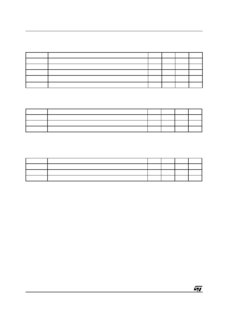
ABSOLUTE MAXIMUM RATINGS (T
CASE
= 25
∞
C)
Symbol
Parameter
Value
Unit
P
DISS
Power Dissipation (T
C
85∞C)*
786
W
I
C
Device Current*
21
A
V
CBO
Collector-Base Voltage
70
V
T
j
Operating Junction Temperature
+250
∞C
T
STG
Storage Temperature
-65 to +200
∞C
THERMAL DATA
R
th(j-c)
Junction -Case Thermal Resistance*
0.21
∞C/W
* Applies only to rated RF amplifier operation: 150 microsec / 10%
AM1214-250
2/4
ELECTRICAL SPECIFICATION (T
CASE
= 25
∞
C)
STATIC
DYNAMIC @ 150 MICROSEC / 10 %
DYNAMIC @ 500 MICROSEC / 10 %
Symbol
Test Conditions
Min.
Typ.
Max.
Unit
BV
CBO
I
C
= 50 mA
I
E
= 0 mA
70
V
BV
CES
I
C
= 50 mA
V
BE
= 0 V
70
V
BV
EBO
I
E
= 20 mA
I
C
= 0 mA
3.5
V
I
CES
V
CE
= 40 V
V
BE
= 0 V
10
mA
h
FE
V
CE
= 5 V
I
C
= 0.5 A
10
Symbol
Test Conditions
Min.
Typ.
Max.
Unit
P
OUT
f = 1215 - 1400 MHz
P
IN
= 40 W
V
CC
= 50 V
300
350
W
C
f = 1215 - 1400 MHz
P
IN
= 40 W
V
CC
= 50 V
40
45
%
G
P
f = 1215 - 1400 MHz
P
IN
= 40 W
V
CC
= 50 V
8.75
9.4
dB
Symbol
Test Conditions
Min.
Typ.
Max.
Unit
P
OUT
f = 1215 - 1400 MHz
P
IN
= 40 W
V
CC
= 42 V
225
250
W
C
f = 1215 - 1400 MHz
P
IN
= 40 W
V
CC
= 42 V
40
45
%
G
P
f = 1215 - 1400 MHz
P
IN
= 40 W
V
CC
= 42 V
7.5
8.0
dB

AM1214-250
4/4
Information furnished is believed to be accurate and reliable. However, STMicroelectronics assumes no responsibility for the consequences
of use of such information nor for any infringement of patents or other rights of third parties which may result from its use. No license is granted
by implication or otherwise under any patent or patent rights of STMicroelectronics. Specifications mentioned in this publication are subject
to change without notice. This publication supersedes and replaces all information previously supplied. STMicroelectronics products are not
authorized for use as critical components in life support devices or systems without express written approval of STMicroelectronics.
The ST logo is registered trademark of STMicroelectronics
Æ
2000 STMicroelectronics - All Rights Reserved
All other names are the property of their respective owners.
STMicroelectronics GROUP OF COMPANIES
Australia - Brazil - China - Finland - France - Germany - Hong Kong - India - Italy - Japan - Malaysia - Malta - Morocco -
Singapore - Spain - Sweden - Switzerland - United Kingdom - U.S.A.
http://www.st.com
