August 1992
S-BAND RADAR APPLICATIONS
RF & MICROWAVE TRANSISTORS
.400 x .500 2L SFL (S138)
hermetically sealed
.
REFRACTORY/GOLD METALLIZATION
.
EMITTER SITE BALLASTED
.
3:1 VSWR CAPABILITY
.
LOW THERMAL RESISTANCE
.
INPUT/OUTPUT MATCHING
.
OVERLAY GEOMETRY
.
METAL/CERAMIC HERMETIC PACKAGE
.
P
OUT
=
105 W MIN. WITH 6.2 dB GAIN
DESCRIPTION
The AM2931-110 is a high power silicon bipolar
NPN transistor specifically designed for S-Band
radar pulsed output and driver applications.
This device is capable of operation over a wide
range of pulse widths, duty cycles and tempera-
tures and can withstand a 3:1 output VSWR. Low
RF thermal resistance, refractory/gold metalliza-
tion, and computerized automatic wire bonding
techniques ensure high reliability and product con-
sistency (including phase characteristics).
The AM2931-110 is supplied in the BIGPAC
TM
Her-
metic M etal/Ceramic package with i nternal
Input/Output matching circuitry, and is intended
for military and other high reliability applications.
PIN CONNECTION
BRANDING
2931-110
ORDER CODE
AM2931-110
ABSOLUTE MAXIMUM RATINGS (T
case
=
25
∞
C)
Symbol
Parameter
Value
Uni t
P
DISS
Power Dissipation*
(T
C
100
∞
C)
375
W
I
C
Device Current*
12
A
V
CC
Collector-Supply Voltage*
48
V
T
J
Junction Temperature (Pulsed RF Operation)
250
∞
C
T
STG
Storage Temperature
-
65 to +200
∞
C
R
TH(j-c)
Junction-Case Thermal Resistance*
0.40
∞
C/W
*Applies only to rated RF amplifier operation
AM2931-110
1. Collector
3. Emitter
2. Base
4. Base
THERMAL DATA
1/4
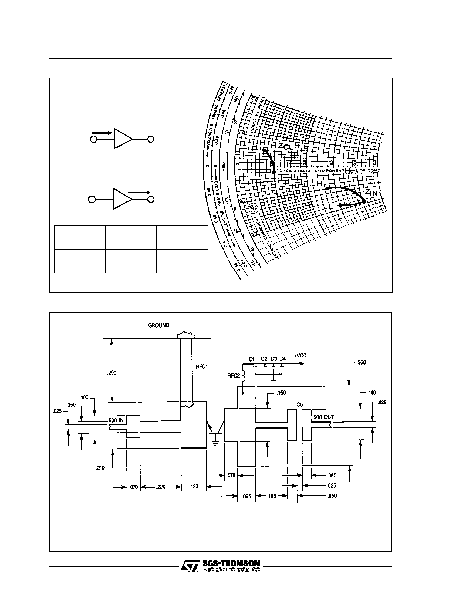
TEST CIRCUIT
All dimensions are in inches.
Substrate material: .025 thick AI
2
O
3
(Er
=
9.6)
C1
: 1500 pF RF Feedthrough
C2
: 1
µ
F, CK06 CapacitorC
C3
: 1
µ
F, Tantalum Capacitor
C4
: 100
µ
F Electrolytic Capacitor, 63V
C5
: 22 pF Chip Capacitor (bridge at location indicated)
RFC1 : Gold Plated Nickel Strap, 0.060 Inch Wide,
0.005 Inch Thick, 0.290 Inch Long
RFC2 : No. 26 Wire, 2 Turn .0.80 Inch I.D.
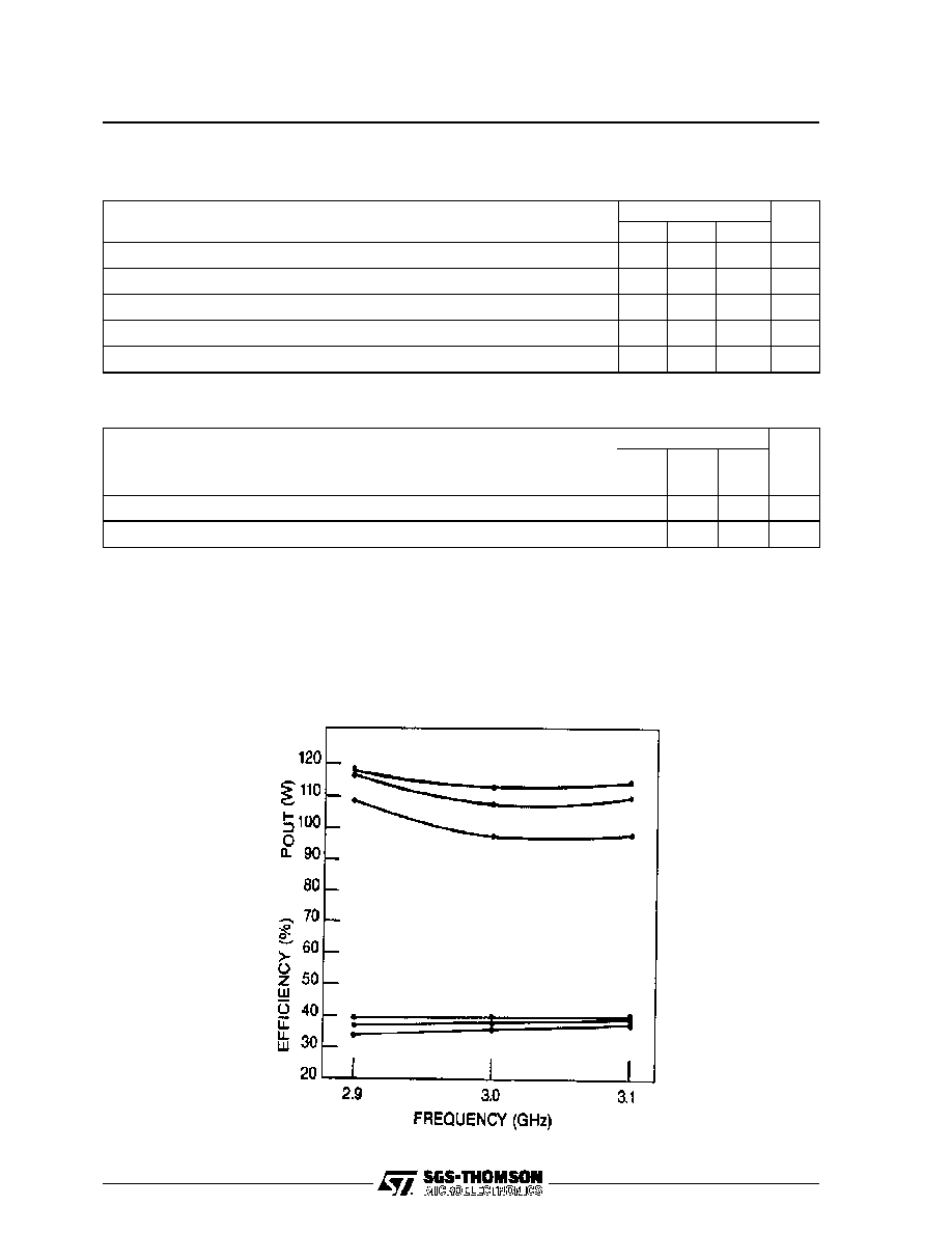
TYPICAL INPUT
IMPEDANCE
TYPICAL COLLECTOR
LOAD IMPEDANCE
P
IN
=
25 W
V
CC
=
42 V
Normalized to 50 ohms
IMPEDANCE DATA
Z
IN
Z
CL
FREQ.
Z
IN
(
)
Z
CL
(
)
L
=
2.9 GHz
15.0
-
j 9.0
5.0
-
j 1.0
M
=
3.0 GHz
20.0
-
j 9.5
4.8 + j 0.5
H
=
3.1 GHz
13.5
-
j 5.0
3.5 + j 2.5
AM2931-110
3/4
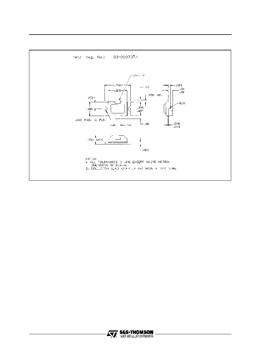
PACKAGE MECHANICAL DATA
Information furnished is believed to be accurate and reliable. However, SGS-THOMSON Microelectronics assumes no responsability for the
consequences of use of such information nor for any infringement of patents or other rights of third parties which may results from its use. No
license is granted by implication or otherwise under any patent or patent rights of SGS-THOMSON Microelectronics. Specifications mentioned
in this publication are subject to change without notice. This publication supersedes and replaces all information previously supplied.
SGS-THOMSON Microelectronics products are not authorized for use as critical components in life support devices or systems without express
written approval of SGS-THOMSON Microelectonics.
©
1994 SGS-THOMSON Microelectronics - All Rights Reserved
SGS-THOMSON Microelectronics GROUP OF COMPANIES
Australia - Brazil - France - Germany - Hong Kong - Italy - Japan - Korea - Malaysia - Malta - Morocco - The Netherlands -
Singapore - Spain - Sweden - Switzerland - Taiwan - Thailand - United Kingdom - U.S.A
AM2931-110
4/4