
L-BAND RADAR APPLICATIONS
RF & MICROWAVE TRANSISTORS
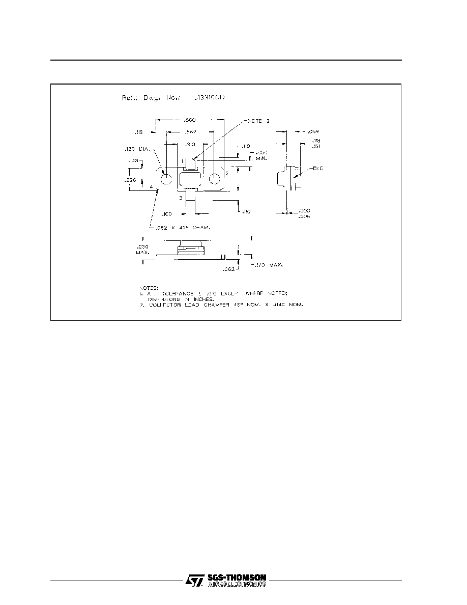
.310 x . 310 2LFL (S064)
hermetically sealed
.
REFRACTORY/GOLD METALLIZATION
.
EMITTER SITE BALLASTED
.
5:1 VSWR CAPABILITY
.
LOW THERMAL RESISTANCE
.
INPUT/OUTPUT MATCHING
.
OVERLAY GEOMETRY
.
METAL/CERAMIC HERMETIC PACKAGE
.
P
OUT
=
14.5 W MIN. WITH 8.6 dB GAIN
DESCRIPTION
The AM81214-015 device is a high power Class C
transistor specifically designed for L-Band Radar
pulsed output and driver applications.
This device is capable of operation over a wide range
of pulse widths, duty cycles, and temperatures and
is capable of withstanding 5:1 output VSWR at rated
RF conditions. Low RF thermal resistance and com-
puterized automatic wire bonding techniques ensure
high reliability and product consistency.
AM81214-015 is supplied in the grounded IMPAC
TM
Hermetic Metal/Ceramic package with internal
input/output matching structures.
PIN CONNECTION
BRANDING
81214-15
ORDER CODE
AM 81214-015
ABSOLUTE MAXIMUM RATINGS (T
case
=
25
∞
C)
Symbol
Parameter
Value
Uni t
P
DISS
Power Dissipation*
(T
C
100
∞
C)
37.5
W
I
C
Device Current*
1.8
A
V
CC
Collector-Supply Voltage*
32
V
T
J
Junction Temperature (Pulsed RF Operation)
250
∞
C
T
STG
Storage Temperature
-
65 to +200
∞
C
R
TH(j-c)
Junction-Case Thermal Resistance*
4.0
∞
C/W
*Applies only to rated RF amplifier operation
AM81214-015
1. Collector
3. Emitter
2. Base
4. Base
THERMAL DATA
August 1992
1/4
.318/
.306
PACKAGE MECHANICAL DATA
Information furnished is believed to be accurate and reliable. However, SGS-THOMSON Microelectronics assumes no responsability for the
consequences of use of such information nor for any infringement of patents or other rights of third parties which may results from its use. No
license is granted by implication or otherwise under any patent or patent rights of SGS-THOMSON Microelectronics. Specifications mentioned
in this publication are subject to change without notice. This publication supersedes and replaces all information previously supplied.
SGS-THOMSON Microelectronics products are not authorized for use as critical components in life support devices or systems without express
written approval of SGS-THOMSON Microelectonics.
©
1994 SGS-THOMSON Microelectronics - All Rights Reserved
SGS-THOMSON Microelectronics GROUP OF COMPANIES
Australia - Brazil - France - Germany - Hong Kong - Italy - Japan - Korea - Malaysia - Malta - Morocco - The Netherlands -
Singapore - Spain - Sweden - Switzerland - Taiwan - Thailand - United Kingdom - U.S.A
AM81214-015
4/4

