.400 x .400 2NLF L (S042)
hermetically sealed
February 3, 1997
S-BAND RADAR APPLICATIONS
RF & MICROWAVE TRANSISTORS
.
REFRACTORY/GOLD METALL IZATION
.
EMITTER SITE BALLASTED
.
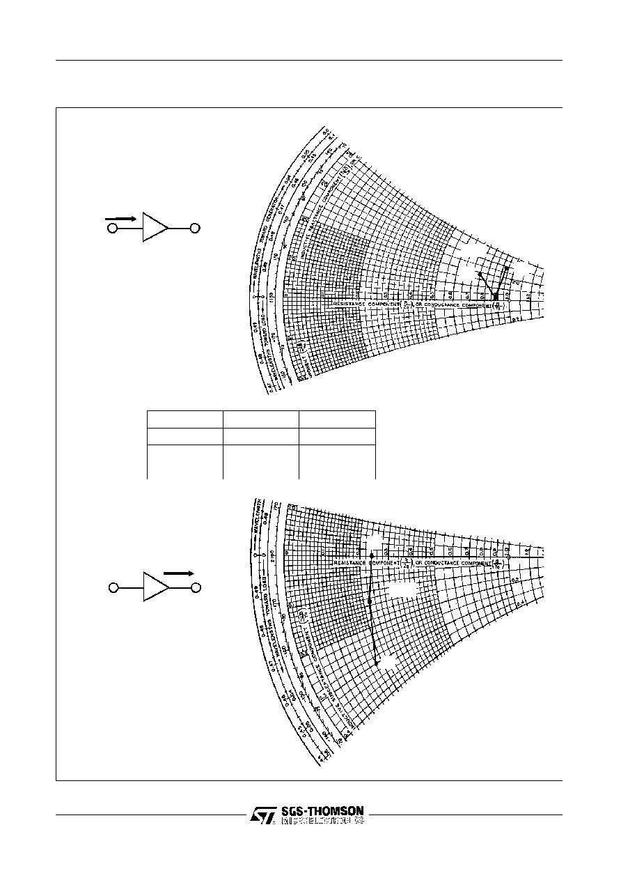
10:1 VSWR CAPABILITY
.
LOW THERMAL RESISTANCE
.
INPUT/OUTPUT MATCHING
.
OVERLAY GEOMETRY
.
METAL/CERAMIC HERMETIC PACKAGE
.
P
OUT
=
1.0 W MIN. WITH 5.2 dB GAIN
DESCRIPTION
The AM83135-001 device is a medium power sili-
con bipolar NPN transistor specifically designed
for S-Band radar pulsed driver applications.
This device is capable of operation over a wide
range of pulse widths, duty cycles and tempera-
tures and can withstand a 10:1 outpu t VSWR.
Low RF thermal resistance, refractory/gold metal-
lization, and automatic wire bonding techniques
ensure high reliability and product consistency.
The AM83135-001 is supplied int the AMPAC
TM
Hermet ic/Ceramic package with internal In-
put/Output impedance matching circuitry, and is
intended for military and other high reliability ap-
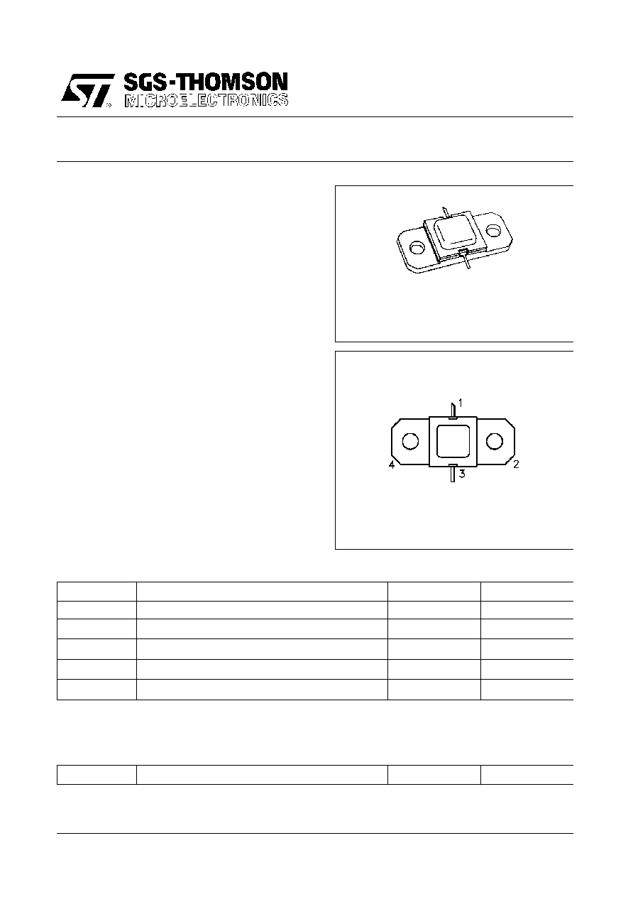
PIN CONNECTION
ABSOLUTE MAXIMUM RATINGS (T
case
= 25
∞
C)
Symbol
Parameter
Value
Un it
P
DISS
Power Dissipation*
(T
C
100
∞
C)
11.5
W
I
C
Device Current*
0.45
A
V
CC
Collector-Supply Voltage*
34
V
T
J
Junction Temperature (Pulsed RF Operation)
250
∞
C
T
STG
Storage Temperature
-
65 to +200
∞
C
R
TH(j- c)
Junction-Case Thermal Resistance*
13.0
∞
C/W
*Applies only to rated RF amplifier operation
AM83135-001
1. Collector
3. Emitter
2. Base
4. Base
THERMAL DATA
BRANDING
83135-1
O RDER CODE
AM83135-001
1/5

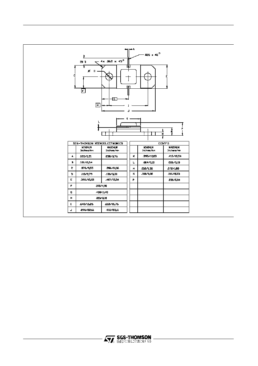
All dimensions are in inches.
Substrate material: .025 thick AI
2
O
3
C1
:
1500 pF RF Feedthrough
C2
:
100 MF Electrolytic
C3
:
100 pF Chip
L1
:
No. 26 Wire, 4 Turn .062 I.D.
L2
:
Printed RF Choke
TEST CIRCUIT
AM83135-001
4/5
Ref.: Dwg. No. 12-0213 rev. A
UDCS No. 1011416
PACKAGE MECHANICAL DATA
Information furnished is believed to be accurate and reliable. However, SGS-THOMSON Microelectronics assumes no responsibility for the
consequences of use of such information nor for any infringement of patents or other rights of third parties which may result from its use.
No license is granted by implication or otherwise under any patent or patent rights of SGS-THOMSON Microelectronics. Specifications
mentioned in this publication are subject to change without notice. This publication supersedes and replaces all information previously
supplied. SGS-THOMSON Microelectronics products are not authorized for use as critical components in life support devices or systems
without express written approval of SGS-THOMSON Microelectronics.
©
1997 SGS-TH OMSON Microelectronics - All Rights Reserved
SGS-THOMSON Microelectronics GROUP OF COMPANIE S
Australia - Brazil - Canada - China - France - Germany - Hong Kong - Italy - Japan - Korea
Malaysia - Malta - Morocco - The Netherlands - Singapore - Spain - Sweden - Switzerland
Taiwan - Thailand - United Kingdom - U.S.A.
AM83135-001
5/5