PRELIMINARY DATA
September 1992
S-BAND RADAR APPLICATIONS
RF & MICROWAVE TRANSISTORS
.310 x .310 2LFL (S064)
hermetically sealed
.
REFRACTORY/GOLD METALLIZATION
.
EMITTER SITE BALLASTED
.
LOW THERMAL RESISTANCE
.
INPUT/OUTPUT MATCHING
.
OVERLAY GEOMETRY
.
METAL/CERAMIC HERMETIC PACKAGE
.
P
OUT
=
30 W MIN. WITH 5.5 dB GAIN
DESCRIPTION
The AM83135-030 device is a high power silicon
bipolar NPN transistor specifically designed for S-
Band radar pulsed output and driver applications.
This device is characterized at 100
µ
sec pulse
width and 10% duty cycle, but is capable of oper-
ation over a range of pulse widths, duty cycles,
and temperatures, and withstand a 3:1 output
VSWR with a + 1 dB input overdrive. Low RF
thermal resistance, refractory/gold metallization,
and computerized automatic wire bonding tech-
niques ensure high reliability and product consist-
ency (including phase characteristics).
The AM83135-030 is supplied in the IMPACTM Her-
metic M etal/Ceramic package with internal
Input/Output impedance matching circuitry, and is
intended for military and other high reliability ap-
plications.
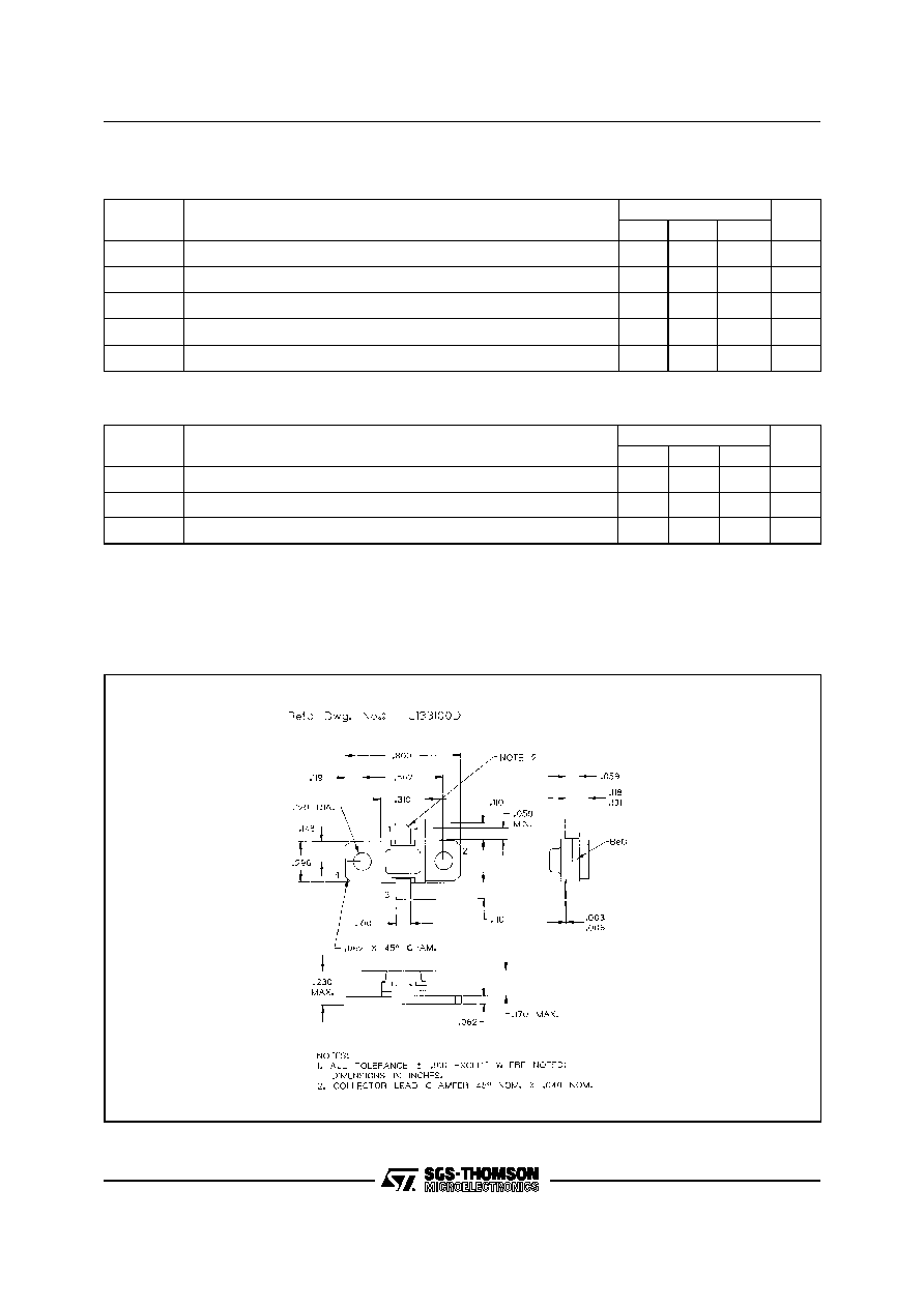
PIN CONNECTION
BRANDING
AM83135-30
ORDER CODE
AM83135-030
ABSOLUTE MAXIMUM RATINGS (T
case
=
25
∞
C)
Symbol
Parameter
Value
Unit
P
DISS
Power Dissipation*
(T
C
50∞C)
133
W
I
C
Device Current*
6.0
A
V
CC
Collector-Supply Voltage*
46
V
T
J
Junction Temperature (Pulsed RF Operation)
250
∞
C
T
STG
Storage Temperature
-
65 to +200
∞
C
R
TH(j-c)
Junction-Case Thermal Resistance*
1.5
∞
C/W
*Applies only to rated RF amplifier operation
AM83135-030
1. Collector
3. Emitter
2. Base
4. Base
THERMAL DATA
1/3

Information furnished is believed to be accurate and reliable. However, SGS-THOMSON Microelectronics assumes no responsability for the
consequences of use of such information nor for any infringement of patents or other rights of third parties which may results from its use. No
license is granted by implication or otherwise under any patent or patent rights of SGS-THOMSON Microelectronics. Specifications mentioned
in this publication are subject to change without notice. This publication supersedes and replaces all information previously supplied.
SGS-THOMSON Microelectronics products are not authorized for use as critical components in life support devices or systems without express
written approval of SGS-THOMSON Microelectonics.
© 1994 SGS-THOMSON Microelectronics - All Rights Reserved
SGS-THOMSON Microelectronics GROUP OF COMPANIES
Australia - Brazil - France - Germany - Hong Kong - Italy - Japan - Korea - Malaysia - Malta - Morocco - The Netherlands -
Singapore - Spain - Sweden - Switzerland - Taiwan - Thailand - United Kingdom - U.S.A
AM83135-030
3/3